Cortex-M3 at 72 MHz — throughput and memory budget
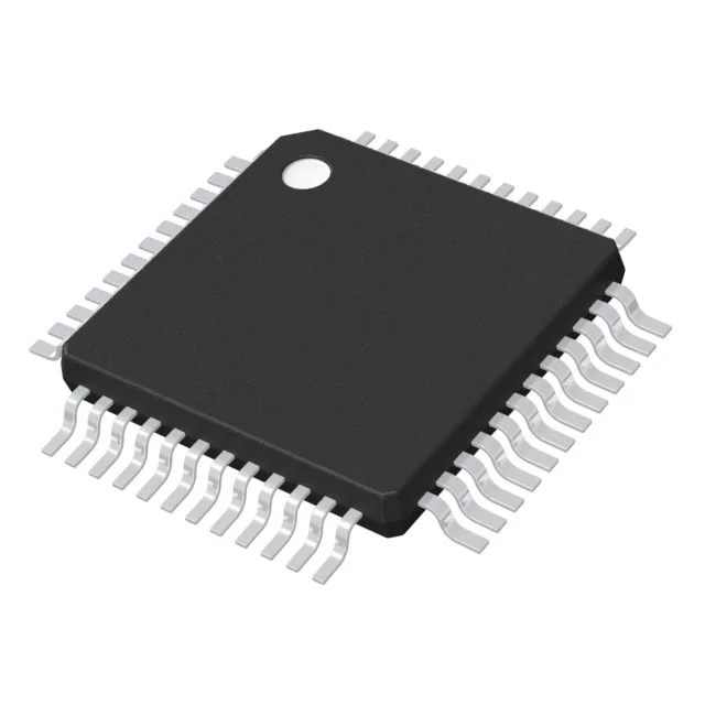
The STM32F103CBT7: On-chip memory is 128 KB of flash and 20 KB of SRAM — the flash holds the application code and constant data; the SRAM budget must cover the stack, heap, and all runtime variables. For a motor-control or sensor-fusion application, 20 KB leaves room for a modest RTOS and a few kB of data buffers. The 48-LQFP package (7x7 mm, 0.5 mm pitch) gives 37 usable I/O — enough for a CAN transceiver, a USB interface, and a handful of sensor inputs without needing a larger package. The exposed pad is not present on this QFP; thermal management relies on the board copper and airflow.
Peripheral set and connectivity for fieldbus and drive control
Built-in peripherals include motor control PWM, DMA, and a temperature sensor — the PWM timers can generate complementary signals with dead-time insertion for a three-phase inverter, and DMA moves ADC results to memory without CPU intervention. Connectivity covers CANbus, USB, I2C, SPI, UART/USART, and IrDA — the CAN interface connects to a fieldbus backbone (e.g., CANopen or J1939), while USB can serve as a virtual COM port for firmware updates or data logging. The 10-channel 12-bit ADC samples at up to 1 µs per conversion — enough for current sensing on a motor drive or for reading multiple analog sensors in a control loop.
Temperature grade, supply, and compliance
The wide range allows direct battery operation (two alkaline cells) without an external LDO. The base product number is STM32F103, so future date-code variants (e.g., -T7 vs -T6) share the same die and peripheral map.