The 24 MHz core speed is the headline parametric for this MCU. At this clock, the Cortex-M3 executes most single-cycle instructions, delivering roughly 0.9 DMIPS/MHz. That's enough for UART polling at 115200 baud, 12-bit ADC sampling in the tens of kilohertz, and PWM generation with sub-microsecond resolution. The flash wait state is zero at 24 MHz, so instruction fetches don't stall.
Memory sizing and peripheral set
64 KB Flash and 8 KB SRAM define the application ceiling. The 8 KB SRAM (organized as 8K x 8) handles moderate data buffers — a 1 KB Modbus register map plus a 2 KB ADC history buffer leaves room for the stack and RTOS kernel objects. The Flash is 64 KB (64K x 8), enough for a FreeRTOS-based application with a USB CDC stack and several peripheral drivers. On the analog side, there are ten 12-bit ADC channels and two 12-bit DAC channels — the DACs are a distinguishing feature versus the STM32F103 which lacks them entirely. The peripheral set includes DMA, a temperature sensor, watchdog timers, and POR/PVD/PDR brown-out management.
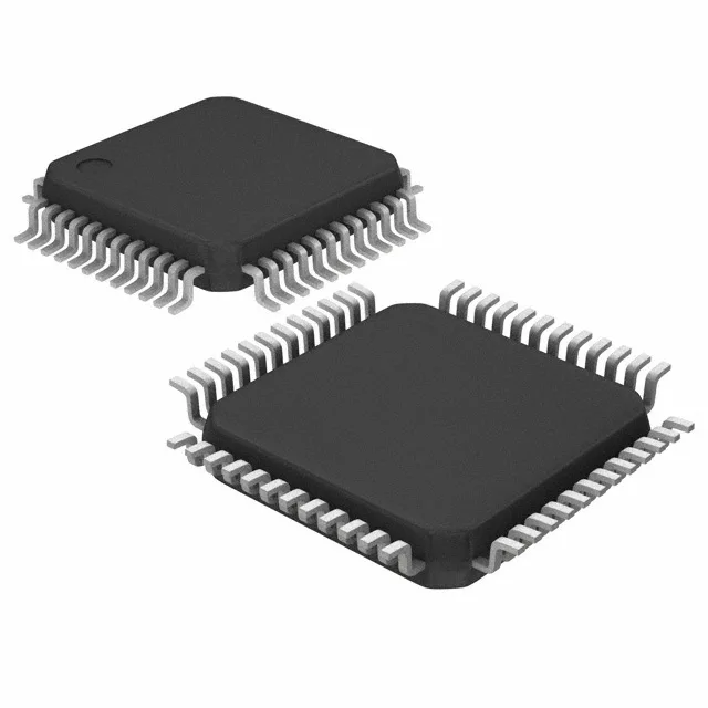
Package and footprint — 48-LQFP
This is a common footprint shared across the STM32F100 value-line density options, so a board layout designed for the 48-LQFP can often accommodate a pin-compatible migration to a higher-density STM32F100 variant without a PCB respin. The 37 I/Os include most peripheral pins brought out; check the alternate function mapping in the datasheet when assigning pin functions to avoid conflicts between SPI and USART on shared pads.