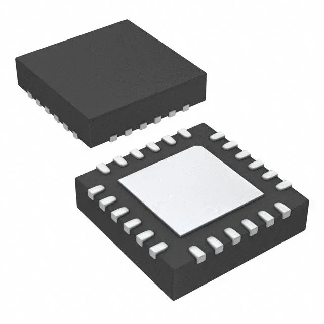
Renesas Electronics 5P49V5913B000NLGI — Clock & Timing ICs

Renesas 5P49V5913B000NLGI Clock Generator, 350 MHz, 24-QFN

MPN5P49V5913B000NLGI
End of Life

Renesas VersaClock® 5 5P49V5913B000NLGI, Clock Generator with PLL, 350 MHz max, HCSL/LVCMOS/LVDS/LVPECL/Crystal input, HCSL/LVCMOS/LVDS/LVPECL output, 1.71V-3.465V supply, -40 to 85°C, 24-VFQFN Exposed Pad (4x4 mm).

$6.92Ref. price · indicative, final on quote
Packaging24-VFQFN Exposed Pad
StockContact for availability
MOQ1 pcs
  • 100% new & originalTraceable channels only — no refurbs, no pulls, no remarked parts.
  • Date & lot codes on quoteStated per line before you commit; label photos on request.
  • MSL-compliant ESD packingMoisture-sealed bags with indicator cards; reels photo-verified.
  • PayPal buyer protectionPay by T/T, PayPal or Payoneer — card payments covered end to end.

Specifications

5P49V5913B000NLGI Technical Specifications
ParameterValue
TypeClock Generator
SeriesVersaClock® 5
Mounting typeSurface Mount
Voltage1.71V ~ 1.89V, 2.375V ~ 2.625V, 3.135V ~ 3.465V
Frequency350MHz
Operating temperature-40°C ~ 85°C (TA)
PLLYes
InputHCSL, LVCMOS, LVDS, LVPECL, Crystal
OutputHCSL, LVCMOS, LVDS, LVPECL
PackageTray
Case24-VFQFN Exposed Pad
Divider (Multiplier)Yes/No
Number of circuits1
Ratio - Input:Output2:2
Differential - Input:OutputYes/Yes

Product details

I/O flexibility — differential and single-ended support

Both the input and output stages support differential signalling (HCSL, LVDS, LVPECL) and single-ended LVCMOS, as indicated by the Yes/Yes differential capability. This means the same part can interface directly with an LVDS oscillator on the input side and drive HCSL-terminated PCIe clocks on the output, without external translation resistors or AC-coupling capacitors beyond what the standard interface requires. The crystal input option also lets the board use a low-cost fundamental-mode quartz rather than a canned oscillator, saving BOM cost and board area.

Lifecycle and sourcing

Renesas lists the 5P49V5913B000NLGI as an Active part (current-production status) with ROHS3 compliance. No pin-compatible second source or direct drop-in replacement from another vendor is documented in the available records, so dual-sourcing would require a functionally equivalent part with a different footprint or programming interface.

Frequently asked questions

Where can I buy 5P49V5913B000NLGI and how is it quoted?

This part is sourced through independent distribution and quoted to order against an RFQ. Availability and current pricing are confirmed at the time of quotation — no stock or price figures are published here.

What is the maximum output frequency of 5P49V5913B000NLGI?

The maximum output frequency is 350 MHz, which covers common reference clocks for Gigabit Ethernet, PCIe, and 10G Ethernet interfaces.

How do I program the output frequencies on VersaClock 5 5P49V5913?

Programming is done via the device's serial interface (I2C or SPI — check the full datasheet for the exact protocol and register map). The PLL dividers and output format registers are configured to set each output's frequency and signal type.