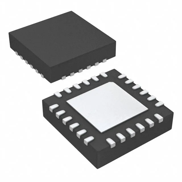
Renesas Electronics 5P49V5925B000NLGI8 — Clock & Timing ICs

Renesas 5P49V5925B000NLGI8 VersaClock 5 Clock Generator

MPN5P49V5925B000NLGI8
End of Life

Renesas VersaClock® 5 5P49V5925B000NLGI8 clock generator, PLL, 200 MHz max output, 2:4 input:output, HCSL/LVCMOS/LVDS/LVPECL/crystal input, LVCMOS output, 1.71V–3.465V supply, -40°C to 85°C, 24-QFN 4x4.

$3.85Ref. price · indicative, final on quote
Packaging24-VFQFN Exposed Pad
StockContact for availability
MOQ1 pcs
  • 100% new & originalTraceable channels only — no refurbs, no pulls, no remarked parts.
  • Date & lot codes on quoteStated per line before you commit; label photos on request.
  • MSL-compliant ESD packingMoisture-sealed bags with indicator cards; reels photo-verified.
  • PayPal buyer protectionPay by T/T, PayPal or Payoneer — card payments covered end to end.

Specifications

5P49V5925B000NLGI8 Technical Specifications
ParameterValue
TypeClock Generator
SeriesVersaClock® 5
Mounting typeSurface Mount
Voltage1.71V ~ 1.89V, 2.375V ~ 2.625V, 3.135V ~ 3.465V
Frequency200MHz
Operating temperature-40°C ~ 85°C (TA)
PLLYes
InputHCSL, LVCMOS, LVDS, LVPECL, Crystal
OutputLVCMOS
PackageTape & Reel (TR); Cut Tape (CT)
Case24-VFQFN Exposed Pad
Divider (Multiplier)Yes/No
Number of circuits1
Ratio - Input:Output2:4
Differential - Input:OutputYes/No

Product details

VersaClock 5 clock generator — what it does on the board

The Renesas 5P49V5925B000NLGI8 is a VersaClock® 5 programmable clock generator with an integrated PLL, designed to synthesize up to four LVCMOS output clocks from a single reference. It accepts differential or single-ended inputs including HCSL, LVCMOS, LVDS, LVPECL, or a crystal, and delivers a clean 200 MHz maximum output frequency. The 2:4 input-to-output ratio means you can distribute two reference sources across four clock lanes, useful for splitting a system clock and a separate Ethernet or PCIe reference without a second PLL IC. Housed in a 24-VFQFN exposed-pad package (4x4 mm body), it fits tight PCIe card or small-form-factor designs where board area is constrained. The industrial temperature range (-40°C to 85°C) covers motor drives, outdoor telecom, and factory automation enclosures where the ambient can swing.

Supply voltage flexibility — three rail domains in one part

This clock generator accepts supply voltages across three distinct ranges: 1.71V to 1.89V (1.8V nominal), 2.375V to 2.625V (2.5V nominal), and 3.135V to 3.465V (3.3V nominal). That triple-domain support means the same BOM line can serve a 1.8V FPGA bank, a 2.5V SerDes reference, or a 3.3V legacy logic system without a separate level translator or regulator — a real advantage when consolidating clock trees across mixed-voltage designs.

PLL and output architecture — what the 200 MHz ceiling means

The integrated PLL multiplies the input reference up to 200 MHz, with a divider chain on the output side (divider present, no multiplier). The single-circuit PLL is sufficient for most single-frequency-domain applications; if you need independent PLLs for asynchronous clock domains, you step up to a multi-PLL VersaClock variant. The LVCMOS-only output means this part drives standard CMOS logic, not differential lines — pair it with a fanout buffer if you need LVDS or LVPECL distribution downstream.

Lifecycle and compliance — active, ROHS3, no LTB risk

It is fully ROHS3 compliant, so it passes EU and global environmental requirements without an exemption certificate. For a production BOM, this part carries no forced-migration risk in the near term — no need to qualify a drop-in replacement unless the design requires dual sourcing.

Package and footprint — 24-QFN with exposed pad

The 24-VFQFN package (4x4 mm, 0.5 mm pitch) has an exposed thermal pad that must be soldered to a ground-plane via array for adequate heat dissipation. The supplier device package is 24-QFN (4x4).

Frequently asked questions

Is 5P49V5925B000NLGI8 RoHS compliant?

Yes, the 5P49V5925B000NLGI8 is ROHS3 Compliant per Renesas lifecycle records, meeting the latest EU RoHS directive without exemptions.

What is the maximum output frequency of 5P49V5925B000NLGI8?

The maximum output frequency is 200 MHz. This ceiling applies to the LVCMOS outputs and is set by the PLL and divider chain. For applications requiring higher frequency differential outputs, a fanout buffer or a different VersaClock variant would be needed.

What are the equivalent parts for 5P49V5925B000NLGI8?

The closest pin-compatible alternative within the VersaClock 5 family is the 5P49V5925B000NLGI (without the trailing '8'), which differs only in packaging or tape/reel format — the functional silicon, PLL architecture, and pinout are identical. For a different output format (e.g., LVDS or HCSL outputs), look at other VersaClock 5 variants with the appropriate output type.