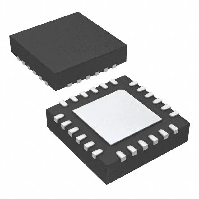
Renesas Electronics 5P49V5901B000NLGI8 — Clock & Timing ICs

Renesas 5P49V5901B000NLGI8 VersaClock 5 Clock Gen, 350MHz

MPN5P49V5901B000NLGI8
End of Life

Renesas Electronics VersaClock® 5 Clock Generator, 5P49V5901B000NLGI8, PLL Yes, 350 MHz max, 2:4 I/O, HCSL/LVDS/LVPECL/LVCMOS, -40 to 85°C, 24-QFN 4x4, Tape & Reel.

$11.35Ref. price · indicative, final on quote
Packaging24-VFQFN Exposed Pad
StockContact for availability
Lead time3-5 Days wk
MOQ1 pcs
  • 100% new & originalTraceable channels only — no refurbs, no pulls, no remarked parts.
  • Date & lot codes on quoteStated per line before you commit; label photos on request.
  • MSL-compliant ESD packingMoisture-sealed bags with indicator cards; reels photo-verified.
  • PayPal buyer protectionPay by T/T, PayPal or Payoneer — card payments covered end to end.

Specifications

5P49V5901B000NLGI8 Technical Specifications
ParameterValue
TypeClock Generator
SeriesVersaClock® 5
Mounting typeSurface Mount
Voltage1.71V ~ 1.89V, 2.375V ~ 2.625V, 3.135V ~ 3.465V
Frequency350MHz
Operating temperature-40°C ~ 85°C (TA)
PLLYes
InputHCSL, LVCMOS, LVDS, LVPECL, Crystal
OutputHCSL, LVCMOS, LVDS, LVPECL
PackageTape & Reel (TR); Cut Tape (CT)
Case24-VFQFN Exposed Pad
Divider (Multiplier)Yes/No
Number of circuits1
Ratio - Input:Output2:4
Differential - Input:OutputYes/Yes

Product details

350 MHz PLL clock generator with 2:4 fanout

The 5P49V5901B000NLGI8 is a VersaClock® 5 clock generator from Renesas, built around a PLL core that synthesizes output clocks up to 350 MHz from any of four input references — HCSL, LVCMOS, LVDS, LVPECL, or a crystal. With a 2:4 input-to-output ratio and differential outputs on all four channels, this part fans out two reference clocks to four independent, phase-aligned copies — enough to drive multiple SerDes transceivers, FPGAs, or Ethernet PHYs from a single PLL bank.

I/O standards and signal integrity

Both the input and output stages support HCSL, LVDS, LVPECL, and LVCMOS — the four most common clock signaling formats in communications and computing. This means the same part can receive a 100 MHz LVDS reference from an FPGA and fan out 156.25 MHz HCSL clocks to a 10G Ethernet PHY without external translators. Because the differential input-to-output path is fully differential (Yes/Yes per the spec), the PLL preserves the low-jitter characteristics of the reference — critical when the output clock is used as a SerDes reference clock where phase noise directly impacts bit-error rate.

RoHS3 compliant (2015/863/EU) with no exemptions — the part is fully lead-free and compatible with standard Pb-free reflow profiles (260°C peak).

Frequently asked questions

What is the difference between 5P49V5901B000NLGI8 and 5P49V5901B616NLGI8?

Both are VersaClock 5 clock generators with the same 24-QFN package, same I/O standards, and same 2:4 fanout. The 5P49V5901B616NLGI8 has a lower maximum output frequency of 200 MHz versus 350 MHz on the 5P49V5901B000NLGI8. They are pin-to-pin compatible — a board designed for one will accept the other without layout changes.

What compliance documentation does Renesas provide for 5P49V5901B000NLGI8?

Renesas provides RoHS3 compliance certification. The part is fully lead-free and meets EU Directive 2015/863. No UL or IEC certification is listed in the available documentation.