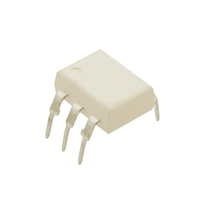
7500Vpk isolation — what it means for the BOM line
The H11A2TVM: The 7500Vpk figure is a peak rating, not a continuous working voltage; for mains-isolation applications you size the creepage and clearance on the PCB to match the working voltage class (IEC 60950 or IEC 62368). With a DC input type and a transistor-with-base output, this part is suited for logic-level signal isolation — the base terminal allows external bias adjustment for switching threshold control, a feature not available on simpler phototransistor couplers that omit the base pin.
Switching speed and CTR — sizing the drive circuit
The current transfer ratio (CTR) is specified at a minimum of 20% at 10 mA forward current — this means with 10 mA through the LED, the phototransistor can sink at least 2 mA at the output. For a given load resistor and output voltage, the CTR sets the minimum LED drive current needed to guarantee the output saturates. The 400 mV Vce(sat) maximum at that drive level means the output pulls within 400 mV of the emitter rail when fully on. Turn-on and turn-off times are 2 µs typical each — this gives a practical switching ceiling around 250 kHz for pulse-width modulation or serial data isolation. For applications requiring faster edge rates, a phototransistor with base access allows a pull-down resistor between base and emitter to speed turn-off, at the cost of reduced effective CTR. The 1.18 V typical forward voltage at the LED means the input side needs a series resistor sized for the desired forward current, up to the 60 mA absolute maximum rating. The 30 V output rating on the phototransistor side covers common logic and control voltages (5 V, 12 V, 24 V) with margin.
A buyer holding an active BOM position for the H11A2TVM should confirm the CTR and isolation requirements before substituting a sibling bin.
Temperature grade and board integration
The through-hole DIP package suits prototype builds, rework-friendly designs, and boards where vibration resistance is less critical than socketability or manual assembly. Supplied in bulk packaging — no tape-and-reel, so pick-and-place assembly requires tube or tray feeding. The 0.400-inch (10.16 mm) body width is wider than the standard 0.300-inch DIP, so verify the PCB footprint matches the wider lead span before layout.