Isolation barrier and signal transfer
The H11A1SR2M is a single-channel phototransistor optoisolator from onsemi that provides 4170Vrms of galvanic isolation between its DC input LED and output phototransistor. This isolation rating suits it for breaking ground loops and protecting low-voltage logic from transient spikes on the field side, common in motor drive feedback, PLC digital inputs, and power-supply error-amplifier paths. With a minimum current transfer ratio of 50% at 10 mA forward current, the LED drive current needed to saturate the output transistor is predictable — budget 10 mA on the input side to guarantee a logic-level output at the collector.
Switching speed and output characteristics
Typical turn-on and turn-off times are both 2 µs, giving a combined propagation delay of about 4 µs. This is fast enough for 100 kHz digital isolation or low-speed serial interfaces like I²C or UART, but not for high-speed fieldbus or gate-drive applications where a logic-output optocoupler with sub-microsecond delay would be needed. The output transistor can handle up to 30 V on the collector and saturates to a maximum of 400 mV at the rated drive current. That 400 mV Vce(sat) means the output can pull a 5 V logic input low enough to register a clean '0' — no level translation needed on the receiving side for standard TTL or CMOS thresholds.
Package, mounting, and environmental range
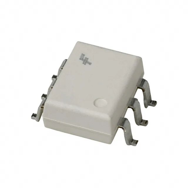
Housed in a 6-SMD gull wing package (supplier device package 6-SMD), the H11A1SR2M is a surface-mount part suited for reflow soldering. The gull wing leads provide good coplanarity and visual solder-joint inspection access — a rework tech can touch up a cold joint with a fine-tip iron without removing the part. The 60 mA absolute maximum forward current on the LED side gives headroom for transient drive spikes, but continuous operation near that limit will degrade the LED over time — stay under 20 mA for long-term reliability.
Lifecycle and compliance
It is fully RoHS3 compliant, meeting the current EU restriction directive without exemptions. The base product number is H11A1, which means this variant (SR2M suffix) is the surface-mount gull wing version on tape-and-reel. If your BOM calls for the through-hole DIP version, the base H11A1 family includes that option, but the SR2M suffix specifically identifies this SMD package.