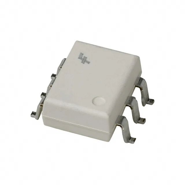
onsemi H11A1SM — Optoisolators
Technical Documents PDF / CAD
RoHS Compliant · Lead-Free EIA-481 Standard
onsemi / Optoisolators

H11A1SM onsemi Optoisolator – 4170Vrms, Transistor Output

MPN H11A1SM
Active Spot Stock · 24-48h Dispatch 100% Original Sealed

onsemi H11A1SM, single-channel optocoupler, 4170Vrms isolation, DC input, transistor with base output, 6-SMD gull wing package, -40°C to 100°C operating range.

In Stock: 24 pcs
MOQ: 1 pcs
Logistics: DHL / FedEx DAP (Global Express · 3-7d) Russia & CIS DDP (Door-to-Door Cleared)
Dispatch: Shenzhen / HK
Unit Price (USD)
$1.29 / pc
Direct Purchase Ready
Volume Pricing Breaks Confirmed upon quotation
1+ pcs
$1.29
10+ pcs
$1.05
Working on a production BOM or have a target unit price? Submit Target Price
Buy Now

$1.29 / ea

24 in stock — maximum per order · 3–4 days lead time

$1.05 / ea from 10 pcs

Upload Full BOM List
[SPEC] Essential Parameters Snapshot Full Specifications (14)
Package / Case 6-SMD, Gull Wing
ALT
Facing long factory lead times or allocation on H11A1SM? Verified pin-compatible alternatives available with active Shenzhen stock and 100% solder-ready footprint match.

Full Technical Specifications

14 Parameters
H11A1SM specifications
Parameter / AttributeSpecification / Value
Input typeDC
Output typeTransistor with Base
MountingSurface Mount
Voltage - isolation4170Vrms
Voltage - output30V
Voltage - forward (Vf)1.18V
Current transfer ratio50% @ 10mA
Current - DC forward (If)60 mA
Operating temperature-40°C ~ 100°C
PackageTube
Case6-SMD, Gull Wing
Channels1
Vce saturation400mV
Turn on (Turn off time)2µs, 2µs
100% Footprint Match · Solder-Ready (No PCB Redesign Needed)

Need Stock or a Drop-in Second-Source for H11A1SM?

Package: DIP-6 · Pin-compatible replacements with immediate Shenzhen spot stock

Footprint Match 98%
Supply Chain & Allocation Reality:

The 4N2x / 4N3x row is the general-purpose opto that predates the PC817 and still fills industrial boards, instruments and old audio gear: a 6-pin DIP with an infrared LED, a phototransistor, and one extra pin the 4-pin generation gave up - the base of the phototransistor, brought out for speed-up tricks and threshold trimming. The family is a CTR ladder wearing four part numbers: 4N25/26 at 20% minimum, 4N27/28 at 10%, and the 4N35/36/37 trio at 100% - one of the highest CTRs of any general-purpose opto, which is why it survives in circuits that need gain more than speed. Substituting within the row is honest work; substituting against the 4-pin PC817 row is the classic socket error.

Verified Pin-Compatible Replacements (4 verified alternatives)

4N25 onsemi / Vishay / Everlight DIP-6
100% Drop-in (Zero Code Change)
Availability & Target Pricing:

The 20% Rung - Same Socket, Real Numbers

Shenzhen Spot Stock (24-48h Dispatch)

Electrical & Core Specs:

The 20% minimum CTR member at 10mA LED current (same bin as the 4N26): the everyday grade of the row, pin-identical to every 4N2x and 4N3x part.

Standard 6-pin opto envelope: 5.3kV-class isolation in the classic parts, 30V-class collector-emitter ratings, pin 6 base exposed.

Compatibility & Drop-In Notes: Substitution inside the row must carry the CTR requirement: a 4N25 (20%) is a genuine downgrade from a 4N35 (100%) in any circuit that relied on the gain - the LED drive may need recomputing. The reverse is free margin.
Package & Solder Footprint: Standard 6-pin DIP; pinout 1 anode, 2 cathode, 3 NC, 4 emitter, 5 collector, 6 base.
Shenzhen Warehouse Stock & MOQ: Stocked across the row; the differences are documented per grade.
4N37 Everlight / Vishay / onsemi DIP-6
100% Drop-in (Zero Code Change)
Availability & Target Pricing:

The 100% CTR Rung

Shenzhen Spot Stock (24-48h Dispatch)

Electrical & Core Specs:

The high-gain member of the row: 100% minimum CTR at 10mA (40% guaranteed across the full temperature range), the reason it appears wherever the driving current must stay small.

Same envelope; isolation figure per the vendor grade (5.3kV class in the classic datasheets).

Compatibility & Drop-In Notes: The honest substitution sentence for this row: going up in CTR is always electrically kind; going down needs the drive budget re-derived - the 10mA figure in the datasheet assumes the LED the original design budgets for.
Package & Solder Footprint: Identical 6-pin DIP footprint.
Shenzhen Warehouse Stock & MOQ: Stocked as the high-gain repair part for marginal-drive circuits.
H11A1 Vishay / onsemi (legacy) DIP-6
Functional Equivalent
Availability & Target Pricing:

The Ancestor Row

Shenzhen Spot Stock (24-48h Dispatch)

Electrical & Core Specs:

The 6-pin row the 4N parts were defined alongside: H11A1 at 50% minimum CTR, H11A5 at 30% - same socket and base pin, its own gain ladder.

Same envelope and isolation class.

Compatibility & Drop-In Notes: In equipment documentation, a service manual often names the H11A part while the board carries a 4N one (or the reverse): the numbers are what matter, the names are lineage.
Package & Solder Footprint: Standard 6-pin DIP pinout.
Shenzhen Warehouse Stock & MOQ: Stocked for legacy equipment; verify markings on older lots.
PC817 Sharp / multiple DIP-4
Functional Equivalent
Availability & Target Pricing:

The 4-Pin Cousin - Different Socket

Shenzhen Spot Stock (24-48h Dispatch)

Electrical & Core Specs:

The 4-pin general-purpose opto of the next generation: same phototransistor idea without the base pin, and its own CTR rank system (A/B/C/D) that replaced the 4N CTR ladder in new designs.

Same functional envelope; 5kV-class isolation in the modern parts.

Compatibility & Drop-In Notes: When a service note says "PC817 replaces 4N35", it means functionally in some circuits - the socket does not agree. Fitting a 4-pin part into a 6-pin footprint needs the adapter or a new layout, and the base-pin behavior is gone either way.
Package & Solder Footprint: DIP-4 against DIP-6: different footprint by construction.
Shenzhen Warehouse Stock & MOQ: The modern volume part; see its own page for the rank system.
Buyer & Quality Checklist for Sourcing Alternatives
  • The CTR minimum is the specification: 4N25/4N26 = 20%, 4N27/4N28 = 10%, 4N35/4N36/4N37 = 100% (40% across the extended range). The 4N3x trio is the same sockets at five times the gain - the direction of every substitution follows this number.
  • Pin 6 (base) distinguishes this row from the 4-pin generation: a base-emitter resistor speeds the transistor up (trading gain for bandwidth), and a small bias trims the threshold. Designs that used it detect a replacement without it immediately - noise and edge behavior change.
  • The 4-pin PC817 row is not the same socket: no base pin, a different rank system (A-D), and a modern isolation class. Functionally comparable in many circuits, mechanically incompatible without an adapter.
  • LED drive is part of the gain budget: the CTR numbers assume 10mA of LED current. A circuit that halved its LED drive for efficiency cannot expect the original switching thresholds from the same grade.
  • The classic 6-pin bodies carry 5.3kV-class isolation figures - verify per vendor and grade; clone rows trade here first.
  • For repair of old gear, read the service manual part against the row: the H11A names and the 4N names cross freely in tables, and the CTR number is the only thing that transfers between them.
Frequently Asked Technical Questions

Q: What is the difference between 4N25 and 4N35?

A: Current transfer ratio: 4N25 is 20% minimum, 4N35 is 100% minimum (40% guaranteed over the extended temperature range). Same 6-pin socket and pinout; the 4N3x part is the high-gain version of the same design.

Q: What is pin 6 on a 4N35 used for?

A: The phototransistor base, brought out for design freedom: a base-emitter resistor speeds up switching, a small bias trims the effective threshold. It is also the physical difference from the 4-pin opto generation.

Q: Can I replace a 4N35 with a PC817?

A: Functionally similar in many circuits, but not socket-compatible - the PC817 is a 4-pin part without the base pin. Fitting one needs an adapter or a new layout, and the base-pin behavior is lost either way.

Technical Details & Description

Device identity and key parametrics

The H11A1SM is a single-channel optocoupler from onsemi with a DC input and a phototransistor output that brings the base terminal out separately. The 4170Vrms isolation rating is the figure a safety engineer checks first — it supports reinforced insulation in mains-referenced circuits such as AC-DC power supplies and motor-drive interfaces. Minimum current transfer ratio is 50% at a forward current of 10 mA. That means the output transistor can sink at least 5 mA when the LED is driven at 10 mA — a straightforward gain to budget into the pull-up resistor on the collector. The typical turn-on and turn-off times are both 2 µs, which is adequate for 50/60 Hz line-frequency isolation and low-speed logic interfaces but not for high-speed data links. Output transistor maximum Vce is 30 V, and the saturation voltage is 400 mV max. The 30 V ceiling suits 24 V industrial logic rails; the low saturation voltage keeps the logic-low level clean when driving a CMOS or TTL input.

Package and mounting for board fit

The H11A1SM is supplied in a 6-SMD gull wing package, surface-mount only. For a BOM position that calls for a through-hole DIP-6, this SMD variant requires a footprint change — confirm the land pattern before committing.

onsemi lists the H11A1SM as Active and ROHS3 compliant.

Frequently asked questions

What is the output type of the H11A1SM?

Transistor with base. The separate base terminal gives the designer the option to bias the transistor for faster switching or to improve noise margin in high-interference environments.

H11A1SM
Verified Allocation
Quote