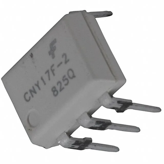
The CNY17F2M is a single-channel optocoupler from onsemi's CNY17F family, built to pass a signal across a 4170 Vrms galvanic barrier. The output is a phototransistor, not a logic gate, so the designer controls the pull-up and the switching threshold. With a 63–125 % current transfer ratio at 10 mA forward current, the CTR bin is tight enough to avoid overdriving a 5 V logic input or leaving it marginal at cold temperature.
Switching speed and saturation — the timing numbers that matter
Turn-on time is 2 µs typical, turn-off 3 µs typical, with rise and fall times of 4 µs and 3.5 µs max. That puts the usable switching frequency around 50–60 kHz for a clean pulse train — fast enough for a PLC input or a gate-drive feedback path, not fast enough for a switching power supply loop. Vce(sat) is 400 mV maximum at the output transistor. That means the collector can pull a 5 V logic input below 0.8 V with margin, even with a 50 mA output load. The 70 V output breakdown gives headroom for 24 V industrial rails or a 48 V telecom bus.
Temperature range and package — where it lives on the board
Rated for –40 to 100 °C, the CNY17F2M covers the thermal envelope of a factory-floor PLC or an outdoor telecom enclosure. The through-hole 6-DIP (0.300", 7.62 mm) footprint is a standard 300-mil DIP — no exotic pad pattern, no reflow profile to tune. The input is DC only — there is no AC-input LED, so the forward current must be unidirectional. If the application needs AC line sensing, look at a zero-crossing or AC-input opto instead.
The BOM line is stable for the foreseeable production horizon. The base product number is CNY17F, so the same die and package family spans multiple CTR bins. The F2 suffix selects the 63–125 % range; the F3 (100–200 %) is a drop-in swap if the design needs more gain. The SR2 suffix variant is the same die in a surface-mount package for reflow assembly.