Through-hole isolation for industrial signal paths
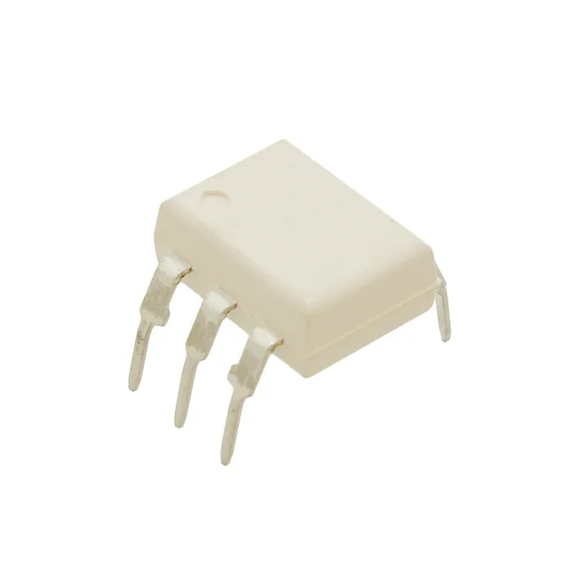
The CNY173TVM is a single-channel optoisolator from onsemi, built around a DC-input LED and a phototransistor output with a base terminal. The 4170Vrms isolation rating makes it a candidate for galvanic barriers in motor-drive feedback, PLC digital inputs, and switch-mode power-supply error-amplifier paths where the primary and secondary sides must not share a ground. The 6-DIP (0.400-inch, 10.16 mm) through-hole package suits wave-solder assembly and prototype rework. The base pin gives the designer the option to add a speed-up capacitor or base resistor for tailoring the switching response — a feature missing on simpler two-pin phototransistor couplers.
CTR window and switching speed for BOM margin
Current transfer ratio is specified at 100% minimum and 200% maximum at If=10 mA. That 2:1 spread is tighter than many general-purpose optos, which can vary 3:1 or more. For the buyer, this means the pull-up resistor on the output side can be sized with less guard-banding, saving board space and reducing component count on the BOM. Turn-on time is 2 µs typical, turn-off 3 µs typical, with rise and fall times of 4 µs and 3.5 µs maximum. At 100 kHz the output waveform will round off, but for 10–50 kHz PWM or serial data at 19.2 kbaud the edges stay clean enough to avoid bit errors. The 400 mV maximum Vce(sat) keeps the output transistor out of deep saturation, which helps maintain those switching times across temperature. Output is rated for 70 V maximum and 50 mA continuous per channel. That voltage ceiling covers 24 V and 48 V industrial rails with margin; the 50 mA current is enough to drive a logic gate input, a relay coil with an external transistor, or a small DC load directly.
Active production with industrial temperature coverage
Sourced per RFQ against BOM quantity.