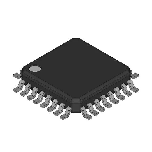
PLL-based clock fanout for 3.3V LVPECL trees
The NXP MPC9993FA is a PLL-based clock driver with bypass, designed to fan out LVPECL reference clocks across a board. It takes up to two LVPECL inputs and distributes them to five LVPECL outputs, with the PLL providing zero-delay or jitter-cleaning capability when enabled, or a clean bypass path when the PLL is not needed. The part runs from a 3.135V to 3.465V supply, making it a direct fit for standard 3.3V clock distribution rails in telecom, networking, and industrial base-station equipment.
200 MHz ceiling and what it buys the design
The 200 MHz maximum frequency sets the upper bound for the clock tree. This covers most 100/125 MHz reference clocks for Ethernet PHYs, FPGAs, and SERDES transceivers, but it won't reach 312.5 MHz or higher rates needed for some 10G+ serial links. If your design needs to distribute a 156.25 MHz or 200 MHz reference to multiple line cards, this part fits. The differential LVPECL I/O keeps signal integrity clean over short board traces, but plan for proper termination — LVPECL requires a DC bias path to VCC - 2V.
Industrial temperature range and deployment context
It is not qualified to AEC-Q100, so it is not a candidate for under-hood automotive or engine-bay environments.
RoHS non-compliance — a sourcing flag
The MPC9993FA is listed as RoHS non-compliant. This means the part uses lead-bearing solder or lead-frame finishes, which is acceptable in military, aerospace, and some industrial applications with exemptions, but it blocks use in EU RoHS-mandated consumer or commercial products. The lifecycle status is Active, so NXP still manufactures it and there is no EOL notice. However, new designs targeting RoHS compliance should look for a lead-free alternative in the same family.