What the 528MHz Cortex-A7 core means for your BOM line
The MCIMX6G2DVM05AB is an NXP i.MX6UL series application processor built around a single ARM Cortex-A7 core clocked at 528MHz — that puts it in the low-power, cost-optimised tier of the i.MX6 family, designed for headless or basic-display embedded systems where a full Cortex-A9 would draw too much current or cost too much.
Package and board-fit — the 289-MAPBGA rework reality
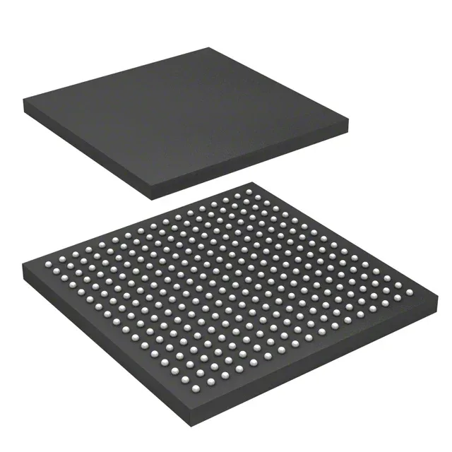
Housed in a 289-MAPBGA (14x14 mm) — that is a 0.8 mm pitch ball grid array, which is hand-reworkable with a decent hot-air station and a stencil, but you will want a pre-bake at 125°C for 12-24 hours if the parts have been sitting in a non-dry-pack environment, because the mould compound absorbs moisture and the 260°C reflow peak can pop the package. The operating temperature range is 0°C to 95°C junction — this is a commercial/industrial-grade part, not automotive; if your enclosure sees ambient above 70°C, you need to calculate the junction rise from the 1.2V core rail current draw to stay under 95°C.
Memory and peripheral fit for a typical embedded system
The RAM controller supports LPDDR2, DDR3, and DDR3L — that gives you flexibility to use whichever memory type your supply chain prefers, though DDR3L at 1.35V is the sweet spot for a single-rail design that also powers the 1.2V, 1.35V, 1.5V, 1.8V, 2.5V, 2.8V, and 3.3V I/O voltages. Two USB 2.0 ports with integrated PHY and two 10/100Mbps Ethernet MACs mean this chip can serve as a dual-Ethernet gateway or an industrial IoT edge node without external USB hubs or PHY chips — just magnetics and an RJ45 connector. The interface list is broad: CAN, EBI/EMI, I2C, I2S, MMC/SD/SDIO, QSPI, SAI, SPI, SSI, S/PDIF, UART — enough to connect a touch controller, audio codec, SD card, and a parallel LCD or LVDS display without an FPGA for glue logic.
Security features — what is on die and what it covers
The security subsystem includes ARM TrustZone, Advanced High-Assurance Boot (A-HAB), Cryptographic Acceleration and Assurance Module (CAAM), Central Security Unit (CSU), Secure JTAG Controller (SJC), and Secure Non-Volatile Storage (SNVS) — this covers secure boot, encrypted firmware storage, and tamper detection without an external secure element.