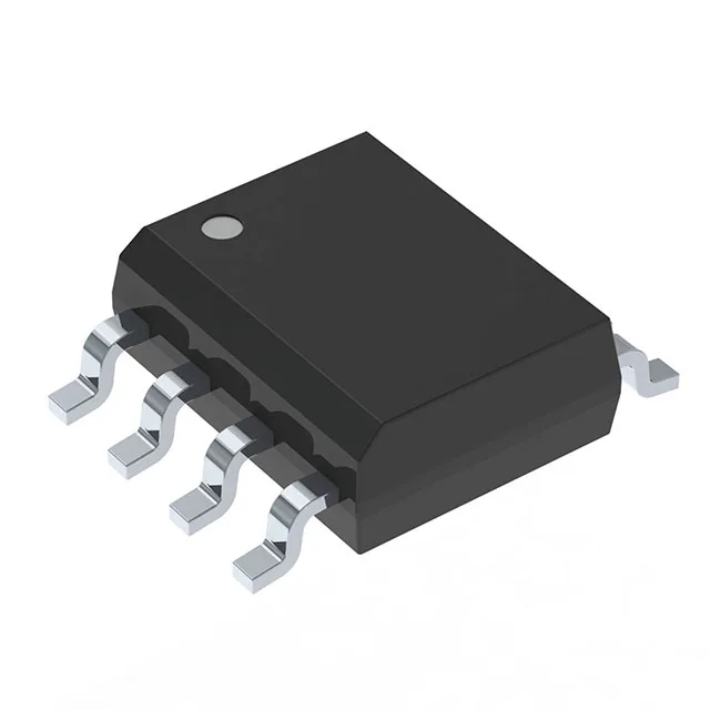
30V, 8.5A N-channel power switch in SO-8
The Infineon IRF7403PBF is a 30V, 8.5A N-channel HEXFET power MOSFET in an industry-standard SO-8 package. It is designed for low-voltage switching applications where conduction loss and thermal performance in a compact footprint are the primary constraints. The part belongs to Infineon's HEXFET series, a mature trench-based process known for consistent Rds(on) and avalanche ruggedness. Maximum on-resistance is 22 mOhm at 4A with a 10V gate drive, and the part is also characterized at 4.5V for logic-level gate drive compatibility. Gate charge is 57 nC at 10V, which is moderate for an SO-8 device and sets the driver current and switching loss budget. The 2.5W power dissipation at 25°C ambient (on standard FR4) sets the thermal design limit for continuous operation.
Gate drive and switching considerations
The IRF7403PBF specifies Rds(on) at both 4.5V and 10V gate drive. At 4.5V, the on-resistance roughly doubles compared to the 10V figure — a detail that matters if the gate is driven from a 5V logic output or a 3.3V rail through a level shifter. The 57 nC gate charge at 10V means the driver must source and sink enough current to hit the target switching speed without excessive crossover loss. Input capacitance is 1200 pF at 25V Vds, which is moderate. For high-frequency switching above a few hundred kHz, the gate charge and Ciss will dominate the driver losses; the part is better suited for load switching, DC-DC converters in the 100-500 kHz range, or as a low-side switch in a motor bridge.
The 2.5W power dissipation at 25°C ambient on a typical FR4 board is a realistic ceiling — for continuous 8.5A, the junction will exceed 150°C unless the PCB copper area is generous or airflow is present. The thermal pad on the SO-8 is the die attach; no exposed pad is available, so the board copper carries the heat. For high-current designs, parallel two devices or use a D-Pak alternative. Mounting is surface-mount only.