Clock distribution hub with spread-spectrum control
The Infineon CY28331OC-2 is a three-in-one clock IC that combines fanout distribution, a multiplexer, and spread-spectrum clock generation in a single 48-BSSOP package. It accepts a crystal input and delivers up to 19 clock outputs at frequencies up to 300 MHz, with differential outputs available on the output side despite a single-ended input. The integrated PLL includes a bypass mode, allowing the system to switch between the internal synthesized clock and an external reference without glitches — useful during test, debug, or failover scenarios where the main PLL must be taken offline while the downstream logic keeps running.
What the 300 MHz ceiling and 1:19 ratio mean for your board
The 300 MHz maximum output frequency sets the upper speed limit for the entire clock tree. At this frequency, the differential outputs (No/Yes input-to-output) maintain signal integrity over longer PCB traces than single-ended routing would allow, reducing jitter accumulation across the 19 fanout paths. A single crystal drives 19 clock loads — the 1:19 input-to-output ratio means one timing source feeds the whole board, eliminating the need for multiple oscillators. The divider/multiplier block (Yes/No) lets you synthesize different frequencies from the same reference, though the part does not multiply the input frequency. The commercial temperature range (0°C to 70°C) limits deployment to controlled indoor environments — not suitable for industrial or automotive enclosures without active cooling.
Package and board-fit considerations
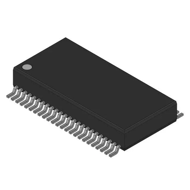
Housed in a 48-BSSOP package with a 0.295-inch (7.50 mm) body width, the CY28331OC-2 requires a surface-mount footprint with a 0.65 mm typical lead pitch. The supplier device package is listed as 48-SSOP, which is the same mechanical outline — confirm the land pattern matches the JEDEC MO-118 standard for SSOP-48 wide-body. Supplied in bulk tube packaging, not tape-and-reel — factor this into your pick-and-place setup if you are running high-volume assembly, as tube-fed feeders may need a changeover from the more common reel-fed lines.