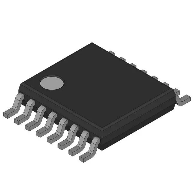
Infineon Technologies CY2213ZC-2 — Clock & Timing ICs

Cypress CY2213ZC-2 Clock Generator, 400 MHz LVPECL, 16-TSSOP

MPNCY2213ZC-2
End of Life

Cypress CY2213ZC-2 Clock Generator, Fanout Distribution, PLL Yes, Input Crystal, Output LVPECL, Frequency Max 400MHz, 1 Circuit, 1:2 Ratio, 3V~3.6V Supply, 16-TSSOP, 0°C~70°C.

$3.3Ref. price · indicative, final on quote
Packaging16-TSSOP (0.173", 4.40mm Width)
StockContact for availability
MOQ1 pcs
  • 100% new & originalTraceable channels only — no refurbs, no pulls, no remarked parts.
  • Date & lot codes on quoteStated per line before you commit; label photos on request.
  • MSL-compliant ESD packingMoisture-sealed bags with indicator cards; reels photo-verified.
  • PayPal buyer protectionPay by T/T, PayPal or Payoneer — card payments covered end to end.

Specifications

CY2213ZC-2 Technical Specifications
ParameterValue
TypeClock Generator, Fanout Distribution
Mounting typeSurface Mount
Voltage3V ~ 3.6V
Frequency400MHz
Operating temperature0°C ~ 70°C (TA)
PLLYes
InputCrystal
OutputLVPECL
PackageBulk
Case16-TSSOP (0.173\", 4.40mm Width)
Divider (Multiplier)No/Yes
Number of circuits1
Ratio - Input:Output1:2
Differential - Input:OutputNo/Yes

Product details

What this clock generator does on your board

The Cypress CY2213ZC-2 is a single-circuit PLL-based clock generator that takes a crystal input and delivers one LVPECL differential output pair, with a second fanout copy, at frequencies up to 400 MHz. It sits in a 16-TSSOP package and runs from a 3V to 3.6V supply. The part is designed for commercial-temperature environments (0°C to 70°C) — think networking gear, test equipment, or base-station timing cards where a clean, low-jitter LVPECL clock is needed from a board-level crystal.

400 MHz LVPECL — what that buys you

The 400 MHz maximum output frequency on the LVPECL pair means this part can clock high-speed SERDES, FPGA gigabit transceivers, or 10G Ethernet PHYs directly. LVPECL swings are small and fast, so the signal integrity budget is tighter than a CMOS clock — keep the trace impedance controlled and the termination close to the receiver. The 1:2 ratio gives you one buffered copy of the PLL output, which is handy for splitting a reference clock between two ASICs or between an FPGA and a PHY without adding a separate fanout buffer.

Crystal input, no differential reference

The input side takes a fundamental-mode crystal — not a CMOS clock or a differential reference. That means your board needs a crystal footprint (parallel resonant, typical load capacitance per the crystal datasheet) between the XIN/XOUT pins. The internal oscillator and PLL do the rest. If your system already has a clean reference clock, you would need a different part with a clock input; this one expects a crystal.

Package and supply — fits standard 16-TSSOP land pattern

The 16-TSSOP package (4.40 mm body width) is a common footprint; the land pattern matches any standard TSSOP-16 layout. Supply range is 3.0V to 3.6V, so a 3.3V rail is the natural fit. No external loop filter components needed — the PLL is fully integrated.

Active lifecycle — no LTB pressure

The CY2213ZC-2 is listed as Active with no end-of-life notification. No last-time-buy planning needed for this BOM line. Note the RoHS status is marked non-compliant, so verify your assembly house's exemption allowance if you are running lead-free processes.

Frequently asked questions

Does CY2213ZC-2 require an external crystal?

Yes, the input is designed for a fundamental-mode crystal. The part does not accept a CMOS clock or differential reference on its input.