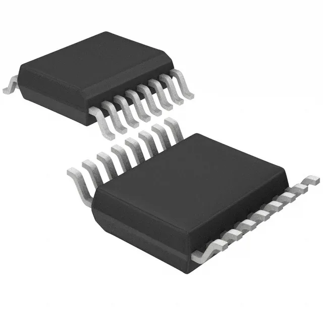
Infineon Technologies CY22393FXI — Clock & Timing ICs

Cypress CY22393FXI Clock Generator, PLL with Bypass, 166 MHz

MPNCY22393FXI
End of Life

Cypress CY22393FXI, Clock Generator with Fanout Distribution, PLL Yes with Bypass, 166 MHz max, 1:6 I/O ratio, LVTTL/Crystal input, CMOS output, 3.135V–3.465V supply, -40 to 85°C, 16-TSSOP.

$20.41Ref. price · indicative, final on quote
Packaging16-TSSOP (0.173", 4.40mm Width)
StockContact for availability
MOQ1 pcs
  • 100% new & originalTraceable channels only — no refurbs, no pulls, no remarked parts.
  • Date & lot codes on quoteStated per line before you commit; label photos on request.
  • MSL-compliant ESD packingMoisture-sealed bags with indicator cards; reels photo-verified.
  • PayPal buyer protectionPay by T/T, PayPal or Payoneer — card payments covered end to end.

Specifications

CY22393FXI Technical Specifications
ParameterValue
TypeClock Generator, Fanout Distribution
Mounting typeSurface Mount
Voltage3.135V ~ 3.465V
Frequency166MHz
Operating temperature-40°C ~ 85°C
PLLYes with Bypass
InputLVTTL, Crystal
OutputCMOS
PackageTube
Case16-TSSOP (0.173\", 4.40mm Width)
Divider (Multiplier)Yes/No
Number of circuits1
Ratio - Input:Output1:6
Differential - Input:OutputNo/No

Product details

What this clock generator does on the board

The Cypress CY22393FXI is a programmable clock generator and fanout distribution IC that takes a single LVTTL or crystal input and delivers six CMOS outputs. Its PLL with bypass lets you choose between a clean, jitter-free crystal-derived clock or a multiplied PLL output, giving the system designer flexibility to clock different speed domains from one reference. The 166 MHz maximum output frequency covers most microcontroller, FPGA, and memory bus clocking needs without pushing into the more expensive high-frequency PLL territory. The 1:6 input-to-output ratio means a single oscillator can drive six loads, saving a clock buffer IC and its associated board space.

166 MHz ceiling — what it buys you on the bus

At 166 MHz, the CY22393FXI can clock a 100 MHz or 133 MHz bus with margin, or drive a 166 MHz DDR memory interface directly. The PLL bypass mode is useful when you need a clean, unmultiplied crystal frequency for a low-jitter reference — say, for an audio codec or an ADC sample clock — while the PLL outputs serve the rest of the board. The trade-off: differential outputs (LVPECL, LVDS) are not available, so this part is limited to single-ended CMOS clock distribution.

Industrial temperature grade — where it lives

Rated for -40°C to 85°C, this part is suited for outdoor telecom cabinets, factory-floor automation controllers, and engine-bay-adjacent electronics that see seasonal temperature swings. The 3.135 V to 3.465 V supply tolerance means it runs cleanly off a standard 3.3 V rail with ±5% regulation, which is the norm for most digital logic and FPGA boards. No separate 1.8 V or 2.5 V rail is needed.

Package and footprint reality

The 16-TSSOP package (4.40 mm body width) is a fine-pitch surface-mount footprint that fits dense layouts without requiring BGA reflow. MSL 3 out of the bag — bake before reflow if the moisture barrier pouch has been open past the floor-life window. The supply decoupling should follow the datasheet's recommended layout: a 0.1 µF ceramic close to each supply pin, with a bulk 10 µF tantalum or MLCC on the input rail.

Lifecycle and sourcing posture

The CY22393FXI is listed as active in production with ROHS3 compliance. For volume production or a BOM line that needs dual-sourcing resilience, the closest functional peer is the CY2305SXI-1HT — a fanout buffer and zero-delay buffer with a 1:5 I/O ratio and 133.33 MHz max frequency, also in a surface-mount package.

Frequently asked questions

What is the maximum frequency of CY22393FXI?

The maximum output frequency is 166 MHz, which covers most microcontroller, FPGA, and memory bus clocking requirements.