PLL with bypass — clock-tree flexibility
The Infineon CY28324PVC is a clock generator IC with an integrated PLL that includes a bypass path. When the PLL is bypassed, the output clock tracks the LVTTL input directly — useful for system debug, frequency margining, or feeding a clean reference into a downstream PLL without the internal loop filter shaping the phase noise. The 1:8 input-to-output ratio means a single LVTTL reference fans out to eight clock outputs, each capable of up to 48 MHz. The outputs are differential, so the part serves designs that need low-jitter clock distribution over longer PCB traces — the differential pair rejects common-mode noise picked up between the source and the load.
48-BSSOP footprint and supply rails
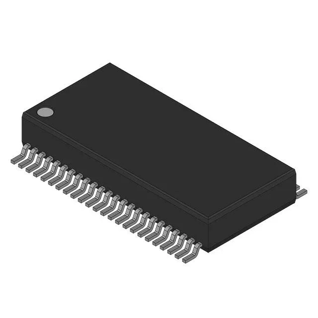
Housed in a 48-BSSOP package with 0.295-inch body width and 7.50 mm pitch, the CY28324PVC demands a standard SSOP land pattern. Supply voltage range is 3.135 V to 3.465 V, a tight 3.3 V ±5 % window. The 3.3 V rail must stay within this band across load transients — a 3.0 V rail from a heavily loaded LDO will push the PLL out of its lock range.
Active lifecycle — RoHS non-compliant
RoHS non-compliant — the part contains lead (Pb) above the 0.1 % threshold. This is a legacy tin-lead finish part, not a RoHS-exempt category. If your BOM requires full RoHS compliance, this part does not meet that requirement and a lead-free alternative must be sourced.
Sourcing posture
Sourced through independent distribution channels. No stock-holding claim is made — each order is quoted to the buyer's quantity.