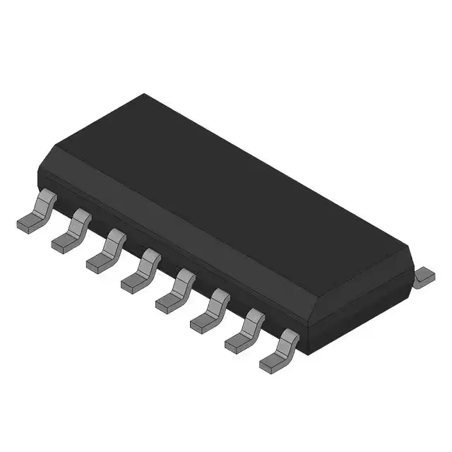
PLL-based clock distribution — 1:8 fanout at 140 MHz
The CY23S08SI-2 is a PLL-based clock driver from Infineon, configured as a Zero Delay Buffer. It accepts a single LVCMOS or LVTTL input and distributes it to eight LVCMOS outputs, with a maximum operating frequency of 140 MHz. The integrated PLL includes a bypass mode, allowing the input clock to pass through unmodified when the PLL is not needed — useful for system-level test or when jitter cleanup is not required.
Industrial temperature range and supply rail
The single-circuit design means one PLL core serves all eight outputs, so the input-to-output phase relationship is consistent across the fanout.
The supplier device package is 16-SOIC. The inputs and outputs are single-ended (non-differential), so no external termination resistors are needed for the clock lines — the LVCMOS levels drive directly into typical FPGA or ASIC clock inputs.
Active lifecycle — compliance flag to note
A critical compliance detail: this part is RoHS non-compliant. For EU-market builds or any project with RoHS-10 substance restrictions, the non-compliant status must be reviewed against the exemption policy or a RoHS-compliant alternative sourced.