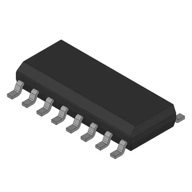
Infineon Technologies CY23S05SC-1H — Clock & Timing ICs

Cypress CY23S05SC-1H Zero Delay Buffer, 133.33 MHz, 8-SOIC

MPNCY23S05SC-1H
End of Life

Cypress CY23S05SC-1H PLL-based Zero Delay Buffer, 133.33 MHz max, 1:5 fanout, 3V–3.6V supply, 8-SOIC (0.154", 3.90mm Width), 0°C to 70°C, RoHS non-compliant.

$2.37Ref. price · indicative, final on quote
Packaging8-SOIC (0.154", 3.90mm Width)
StockContact for availability
MOQ1 pcs
  • 100% new & originalTraceable channels only — no refurbs, no pulls, no remarked parts.
  • Date & lot codes on quoteStated per line before you commit; label photos on request.
  • MSL-compliant ESD packingMoisture-sealed bags with indicator cards; reels photo-verified.
  • PayPal buyer protectionPay by T/T, PayPal or Payoneer — card payments covered end to end.

Specifications

CY23S05SC-1H Technical Specifications
ParameterValue
TypeZero Delay Buffer
Mounting typeSurface Mount
Voltage3V ~ 3.6V
Frequency133.33MHz
Operating temperature0°C ~ 70°C (TA)
PLLYes with Bypass
OutputClock
PackageBulk
Case8-SOIC (0.154\", 3.90mm Width)
Divider (Multiplier)No/No
Number of circuits1
Ratio - Input:Output1:5
Differential - Input:OutputNo/No

Product details

What the CY23S05SC-1H does on your board

The Cypress CY23S05SC-1H is a PLL-based zero delay buffer that takes one clock input and distributes it to five outputs with near-zero propagation delay. It integrates a phase-locked loop with bypass mode, so you can either clean up jitter from the incoming clock or pass the reference straight through when the PLL is not needed. The 1:5 fanout ratio is sized for driving multiple loads on a single PCB — think FPGA reference clocks, Ethernet PHY inputs, or multiple ADC sampling clocks — without adding skew.

133.33 MHz and the PLL bypass — what they mean for timing closure

The maximum output frequency is 133.33 MHz. The PLL with bypass gives two operating modes: with the PLL engaged, output edges align to the input with zero delay; with bypass active, the PLL is shut down and the input clock feeds straight through to the outputs.

Temperature grade and package — where it fits

Rated for 0°C to 70°C ambient, this part is intended for commercial indoor equipment — office networking gear, test equipment, consumer electronics, and telecom line cards in climate-controlled environments. The 8-SOIC package (3.90 mm body width) is a standard surface-mount footprint that reflows easily and is compatible with most PCB assembly lines. The supplier device package is also 8-SOIC, so no footprint mismatch between the case and the recommended land pattern.

RoHS non-compliant — plan for it

This part is marked RoHS non-compliant, meaning it contains lead (Pb) in the solder finish or die attach. For EU markets or any assembly that must meet RoHS exemption rules, you will need to verify whether your end product qualifies for an exemption (e.g., for high-reliability or server applications).

How it compares to the CY2305SXI-1HT

The closest functional peer is the CY2305SXI-1HT. Both are PLL-based zero delay buffers with the same 1:5 fanout, 133.33 MHz maximum frequency, and 3.0 V supply. The key difference is the operating temperature range: the CY23S05SC-1H is rated for 0°C to 70°C (commercial), while the CY2305SXI-1HT covers -40°C to 85°C (industrial).

Frequently asked questions

Does the CY23S05SC-1H have PLL bypass?

Yes, the PLL includes a bypass mode. When bypass is enabled, the PLL is shut down and the input clock passes directly to the outputs, saving power and avoiding lock-time delays during startup.

What is the CY23S05SC-1H equivalent?

The closest functional equivalent is the CY2305SXI-1HT, which offers the same 1:5 fanout, 133.33 MHz maximum frequency, and 3.0 V supply, but with an industrial temperature range (-40°C to 85°C) and Tape & Reel packaging. If your application requires extended temperature or reel format, that is the direct alternative.