Supply voltage range and logic compatibility
The SN74AUP2G125DQER: The 0.8V to 3.6V supply range means this buffer works with 1.2V, 1.8V, 2.5V, and 3.3V logic families without a level translator on the output side — handy when bridging a low-voltage MCU to a higher-voltage peripheral. At 1.8V it is fully specified, so it slots directly into modern low-power FPGA or MCU I/O banks without extra regulation.
3-state outputs and bus isolation
The 3-state outputs let you disable the buffer's drive, putting the output pins into a high-impedance state. That is useful on shared data buses where multiple devices take turns driving the line — the buffer goes quiet when not selected.
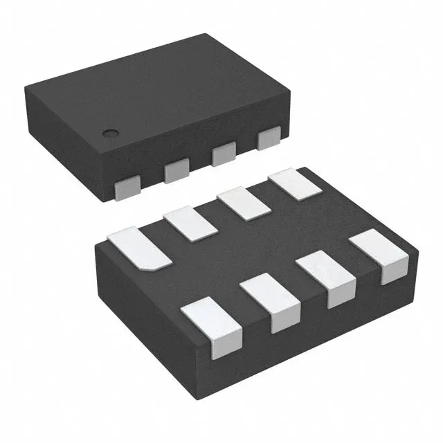
The 8-X2SON (1.4x1.0 mm) package is a leadless, surface-mount package with a 0.5 mm pitch. It requires a reflow oven for assembly — not a hand-solder job in the field. The small footprint saves space but calls for careful PCB layout and a stencil for solder paste. The part is also available in Cut Tape (CT) for prototyping and Tape & Reel (TR) for production runs.