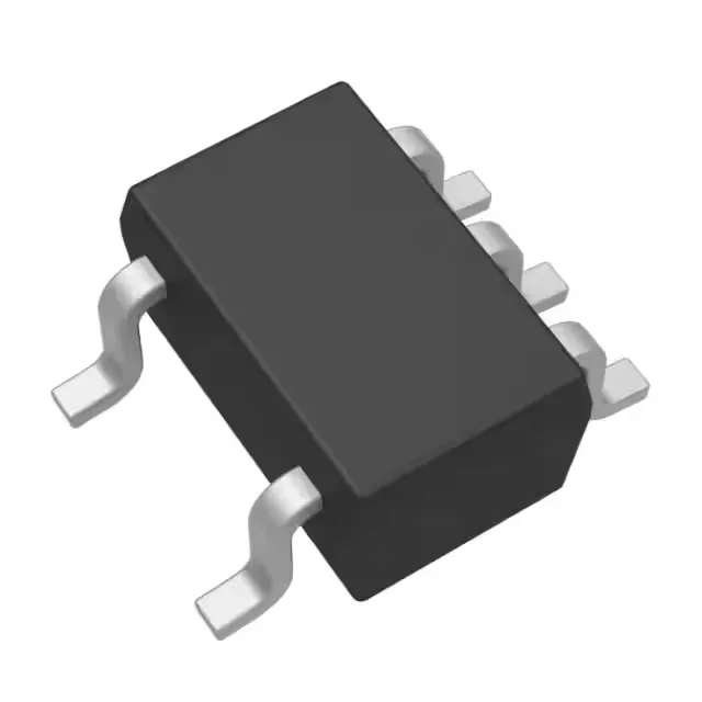
Single 2-input NAND in the 74AUP family
The SN74AUP1G00DCKR is a single 2-input NAND gate from Texas Instruments' 74AUP series — the ultra-low-power CMOS logic family. It packs one gate in a 5-pin SC-70-5 (SOT-353) package, drawing just 500 nA quiescent current maximum. Supply voltage spans 0.8 V to 3.6 V, making it suitable for battery-operated and low-voltage core logic where every nanoamp matters. The output can source or sink 4 mA, enough to drive a single CMOS load or a short PCB trace.
Propagation delay and signal-integrity budget
Maximum propagation delay is 6.5 ns at 3.3 V with a 30 pF load — this sets the data-rate ceiling for the gate in a typical bus. The delay rises at lower supply voltages; at 1.8 V the gate slows, so budget the full 0.8 V–3.6 V range when estimating timing margin. Input logic thresholds are specified as voltage ranges: low level 0.7 V to 0.9 V, high level 1.6 V to 2.0 V. These shift with supply, so the gate's noise immunity is proportional to VCC — at 1.2 V the low threshold is tighter than at 3.3 V.
Active production, ROHS3, industrial temp
Sourced to order against your BOM quantity — availability and current pricing confirmed at RFQ. No pin-compatible second-source is listed; the 74AUP family is TI-specific, so any replacement would require a board spin or a different package.