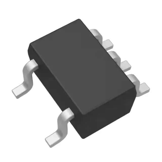
Texas Instruments SN74AUP1G00DCKT — Analog & Data Acquisition

SN74AUP1G00DCKT 74AUP NAND Gate, 500 nA quiescent, SC-70-5

MPNSN74AUP1G00DCKT
End of Life

Texas Instruments 74AUP series, SN74AUP1G00DCKT, single 2-input NAND gate, 0.8 V to 3.6 V supply, 500 nA max quiescent, 6.5 ns propagation delay at 3.3 V / 30 pF, SC-70-5 package, -40°C to 85°C.

$1.07Ref. price · indicative, final on quote
Packaging5-TSSOP, SC-70-5, SOT-353
StockContact for availability
MOQ1 pcs
  • 100% new & originalTraceable channels only — no refurbs, no pulls, no remarked parts.
  • Date & lot codes on quoteStated per line before you commit; label photos on request.
  • MSL-compliant ESD packingMoisture-sealed bags with indicator cards; reels photo-verified.
  • PayPal buyer protectionPay by T/T, PayPal or Payoneer — card payments covered end to end.

Specifications

SN74AUP1G00DCKT Technical Specifications
ParameterValue
Series74AUP
Logic typeNAND Gate
Mounting typeSurface Mount
Voltage0.8V ~ 3.6V
Current - quiescent500 nA
Current - output high, low4mA, 4mA
Number of inputs2
Operating temperature-40°C ~ 85°C
PackageTape & Reel (TR); Cut Tape (CT)
Case5-TSSOP, SC-70-5, SOT-353
Number of circuits1
Input logic level - low0.7V ~ 0.9V
Input logic level - high1.6V ~ 2V
Max propagation delay @ v, max CL6.5ns @ 3.3V, 30pF

Product details

Single NAND gate for power-sensitive glue logic

The Texas Instruments SN74AUP1G00DCKT is a single 2-input NAND gate from the 74AUP ultra-low-power logic family. It operates from 0.8 V to 3.6 V and draws a maximum quiescent current of 500 nA, making it a fit for battery-powered, portable, and always-on circuits where every microamp counts. The SC-70-5 package keeps board area small, and the -40°C to 85°C range covers most industrial and outdoor telecom enclosures.

500 nA quiescent — what it means for a battery budget

The 500 nA maximum quiescent current is the headline spec. In a system that spends most of its time in a low-power idle state — a sensor node, a handheld controller, a remote I/O module — this gate adds negligible drain to the battery budget. The wide supply range (0.8 V to 3.6 V) lets it run directly from a single Li-ion cell or a 3.3 V rail without a regulator, and it can interface with both 1.8 V and 3.3 V logic domains without level translation.

6.5 ns propagation delay — timing margin check

At 3.3 V with a 30 pF load, the maximum propagation delay is 6.5 ns. That is fast enough for general-purpose glue logic, enable gating, and control signal conditioning in systems running at a few tens of megahertz. It is not a high-speed clock buffer — if your path needs sub-3 ns, look at the 74LVC or 74AHC families. The output drive is 4 mA source and sink, adequate for driving a single CMOS load or a short PCB trace.

SC-70-5 — rework and inspection notes

The SC-70-5 (SOT-353) package is 2.0 mm × 1.25 mm with a 0.65 mm pin pitch. It is small enough that hand-soldering is possible with a fine tip and magnification, but the part is light and can shift during reflow if the solder paste is over-applied. The part is surface-mount only — no through-hole variant exists.

Active lifecycle and compliance

It is ROHS3 compliant, so it meets the current EU and global restriction requirements. No AEC-Q automotive qualification is listed — this is an industrial-temperature-grade part, not for under-hood or chassis-domain automotive use.

Frequently asked questions

Will SN74AUP1G00DCKT drop into a board designed for SN74LVC2G00DCT3 without rewiring?

No. The SN74LVC2G00DCT3 is a dual NAND gate in an 8-pin SOT-23 package, while the SN74AUP1G00DCKT is a single gate in a 5-pin SC-70. The pin counts and footprints are different — a board designed for the dual gate would need a layout change to use the single gate.