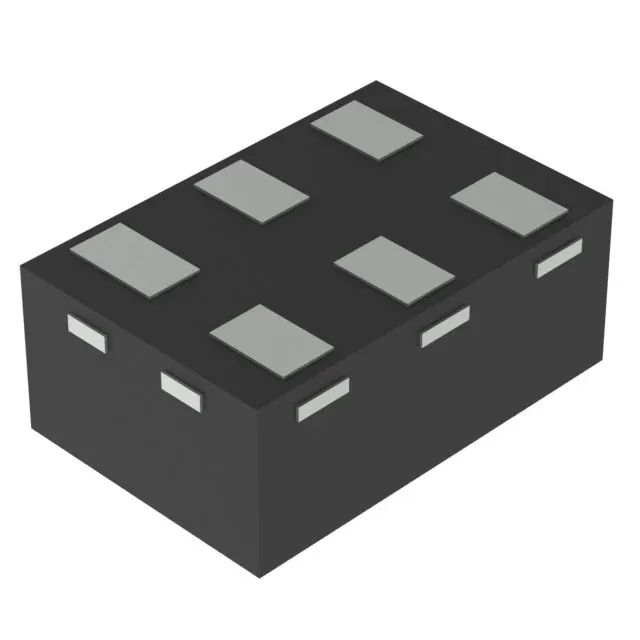
Package and board integration — 6-UFDFN (1.45x1 mm)
The SN74AUP1G00DRY2: The 6-UFDFN package (supplier device package 6-SON, 1.45x1 mm) is a tiny, leadless package with a 0.5 mm pitch. This footprint demands a controlled soldering profile and careful PCB layout — the exposed pad on the bottom requires a thermal land pattern on the board for proper solder joint formation, and the narrow pitch limits trace escape routing to inner layers on dense boards. The package is supplied in Tape & Reel or Cut Tape options, which affects pick-and-place setup and reel quantity for production runs.
Supply voltage range and quiescent current — the battery-life story
The 0.8V to 3.6V supply range lets this gate run directly from a single Li-ion cell (3.0-4.2V) or a pair of alkaline cells (1.8-3.0V) without an intermediate regulator. The 500 nA maximum quiescent current means the gate's own draw is negligible in an always-on sense path — a wearable or IoT sensor that spends most of its life asleep loses less than 0.5 µA to this single gate. At the low end of the supply range (0.8V), the gate still operates but with wider input thresholds — the low-level threshold is 0.7V max and the high-level threshold is 1.6V min at 3.3V, so at lower Vcc the noise margin shrinks. Designers should verify the input signal swing against the datasheet's threshold curves at their operating voltage.
Propagation delay and output drive — what 6.5 ns and 4 mA mean on the bench
The 6.5 ns max propagation delay at 3.3V with a 30 pF load is the time from input crossing the threshold to output crossing 50% of Vcc. This is fast enough for control signals (GPIO toggling, reset lines, enable signals) but not for high-speed data buses — the delay plus the output rise time into the load capacitance sets the maximum toggle rate, which is well below 100 MHz for any real trace length. The 4 mA output drive at both high and low levels is typical for the 74AUP family. This drives one or two standard CMOS inputs but will struggle with long PCB traces (high capacitance) or multiple fan-out loads — a 30 pF load at 3.3V and 10 MHz draws about 1 mA dynamic current, so the 4 mA limit is comfortable for light loads but not for driving a bus or a long cable.
Lifecycle and compliance — active production, no obsolescence risk
This gate is safe for new designs and ongoing production without a forced migration. The device is ROHS3 compliant, meeting the current restriction on lead and other hazardous substances.