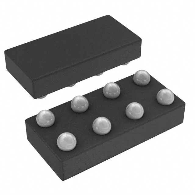
Dual AND gate in a 1.9x0.9 mm footprint
The SN74AUP2G08YZPR is a dual 2-input AND gate from TI's 74AUP series, packaged in an 8-DSBGA (1.9x0.9 mm). It operates from 0.8V to 3.6V supply, drawing just 500 nA quiescent current max. Propagation delay is 6.7 ns at 3.3V with a 30 pF load — fast enough for most general-purpose logic gating in battery-powered or low-voltage systems. The DSBGA package means the solder balls are the only mechanical connection; board-level reliability depends on the PCB land pattern matching TI's recommended footprint and the reflow profile. No underfill is required for typical portable applications, but mechanical shock specs should be reviewed for high-vibration environments.
Supply range and output drive
Supply voltage spans 0.8V to 3.6V, covering single-cell battery operation (0.9V nominal) through standard 3.3V rails. The input logic thresholds scale with VCC: low level is 0.7V to 0.9V, high level is 1.6V to 2V — these are not fixed TTL levels, so the driving device must swing rail-to-rail or close to it. Output current capability is 4 mA source and 4 mA sink at the rated voltage — sufficient for driving a single CMOS load or a low-power LED indicator, but not for heavy fan-out. The 500 nA quiescent current is the standby draw; dynamic current scales with switching frequency and load capacitance. Operating temperature range is -40°C to 85°C, which covers industrial and commercial environments but not extended automotive under-hood conditions.
CT is for prototype or low-volume builds.