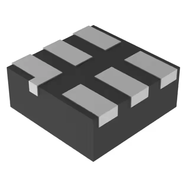
Texas Instruments SN74AUP1G00DSF2 — Analog & Data Acquisition

SN74AUP1G00DSF2 NAND Gate, 0.8-3.6V, 6-XFDFN

MPNSN74AUP1G00DSF2
End of Life

Texas Instruments 74AUP series single 2-input NAND gate, SN74AUP1G00DSF2, 0.8V-3.6V supply, 500 nA quiescent, 6-XFDFN package, surface mount.

$0.6Ref. price · indicative, final on quote
Packaging6-XFDFN
StockContact for availability
Lead timeIn Stock wk
MOQ1 pcs
  • 100% new & originalTraceable channels only — no refurbs, no pulls, no remarked parts.
  • Date & lot codes on quoteStated per line before you commit; label photos on request.
  • MSL-compliant ESD packingMoisture-sealed bags with indicator cards; reels photo-verified.
  • PayPal buyer protectionPay by T/T, PayPal or Payoneer — card payments covered end to end.

Specifications

SN74AUP1G00DSF2 Technical Specifications
ParameterValue
Series74AUP
Logic typeNAND Gate
Mounting typeSurface Mount
Voltage0.8V ~ 3.6V
Current - quiescent500 nA
Current - output high, low4mA, 4mA
Number of inputs2
Operating temperature-40°C ~ 85°C
PackageTape & Reel (TR); Cut Tape (CT)
Case6-XFDFN
Number of circuits1
Input logic level - low0.7V ~ 0.9V
Input logic level - high1.6V ~ 2V
Max propagation delay @ v, max CL6.5ns @ 3.3V, 30pF

Product details

Single 2-input NAND in the 74AUP family

The SN74AUP1G00DSF2 is a single 2-input NAND gate from Texas Instruments' 74AUP series — the ultra-low-power logic family that draws just 500 nA quiescent current maximum, making it a fit for battery-operated and always-on circuitry where every microamp counts. The 6-XFDFN package (1x1 mm body, 6-SON) keeps the footprint minimal — useful when board real estate is tight and the gate sits close to the load it drives.

What the 6.5 ns propagation delay means for timing

Maximum propagation delay is 6.5 ns at 3.3V with a 30 pF load — this sets the data-rate ceiling through the gate. At lower supply voltages the delay increases, so the usable toggle rate drops; at 1.2V the delay is roughly double the 3.3V figure. The 4 mA output drive at both high and low levels is enough to switch a downstream CMOS input or a short PCB trace, but not a long cable or a high-capacitance bus — plan a buffer if the fan-out exceeds a few gates.

Frequently asked questions

Where can I buy SN74AUP1G00DSF2?

The SN74AUP1G00DSF2 is available to order through independent distribution channels.

What is the difference between SN74AUP1G00DSF2 and SN74AUP1G00DCK?

The difference is the package: SN74AUP1G00DSF2 comes in a 6-XFDFN (1x1 mm SON), while the DCK suffix indicates a 5-pin SC-70 package. The logic function and electrical specs are the same — the choice is driven by board footprint and assembly process.

Can I use SN74AUP1G00DSF2 as a level shifter?

A single NAND gate can be configured as a level translator by tying one input to a reference voltage and using the other as the signal input, but it is not a dedicated level shifter. The 0.8V to 3.6V supply range means the output swings rail-to-rail, so the translated signal matches the supply voltage.