J-FET input, hermetically sealed — what this op-amp is for
The 5962-9080701M2A is a single-channel J-FET input operational amplifier in a hermetic 20-CLCC ceramic package, designed for precision analog signal conditioning in environments that demand wide temperature tolerance and long-term reliability. Its J-FET input stage delivers an input bias current of just 4 pA, making it suitable for high-impedance sensor interfaces, photodiode amplifiers, and integrator circuits where bias current errors must be minimised. The gain-bandwidth product of 2 MHz and slew rate of 3.4 V/µs place it in the moderate-speed class, adequate for audio-frequency processing, slow control loops, and data-acquisition front-ends below a few hundred kilohertz. The output can source or sink 80 mA, enough to drive modest loads or feed into an ADC input directly.
Military temperature grade and hermetic package — deployment context
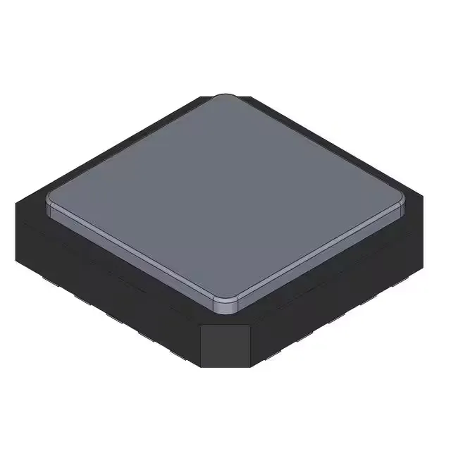
The 20-CLCC package is a ceramic leadless chip carrier, hermetically sealed against moisture and contamination, and the supplier device package is specified as 20-LCCC with a body size of 8.89 x 8.89 mm.
The supply span runs from 7 V minimum to 36 V maximum, giving flexibility for single-supply designs (e.g., a 12 V or 24 V industrial rail) or split supplies like ±5 V to ±18 V. The 600 µV maximum input offset voltage is typical for a J-FET op-amp of this generation — adequate for 12-bit systems with gain below 100, but a precision design targeting better than 0.1% accuracy at high gain should budget for offset trimming or select a lower-offset grade. Supply current is 290 µA, which is modest for a single-channel device and keeps the thermal rise in the hermetic package manageable even at high ambient temperatures.
For a military-grade hermetic part, this is a strong signal: the manufacturer continues to support the die and package combination, and the supply chain for the ceramic substrate and lid seal is maintained.