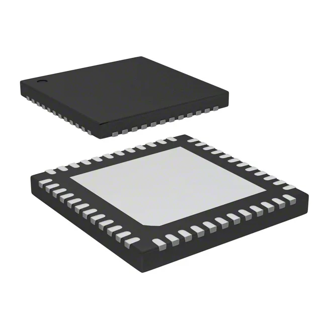
STMicroelectronics STM32F103CBU6 — Microcontrollers & Processors (MCU / MPU / DSP)

STM32F103CBU6 STM32F1 MCU, 72MHz, 128KB Flash, 48-UFQFPN

MPNSTM32F103CBU6
Active

STMicroelectronics STM32F1 ARM Cortex-M3 32-bit MCU, STM32F103CBU6, 72MHz, 128KB FLASH, 20K x 8 RAM, 37 I/O, 48-UFQFPN (7x7 mm) exposed pad, -40 to +85°C, tray.

$6.8400Ref. price · indicative, final on quote
Packaging48-VFQFN Exposed Pad
RoHSROHS3 Compliant
SeriesSTM32F1
Independent supplier — new & surplus stockAuthenticity-screened · ESD-safe packingListing updated Aug 2026

Specifications

STM32F103CBU6 specifications
ParameterValue
SeriesSTM32F1
MountingSurface Mount
Oscillator typeInternal
Program memory typeFLASH
Voltage - supply (Vcc (Vdd))2V ~ 3.6V
Operating temperature-40°C ~ 85°C (TA)
Speed72MHz
PackageTray
RAM size20K x 8
Core size32-Bit Single-Core
PeripheralsDMA, Motor Control PWM, PDR, POR, PVD, PWM, Temp Sensor, WDT
ConnectivityCANbus, I²C, IrDA, LINbus, SPI, UART/USART, USB
Number of i (O)37
Core processorARM® Cortex®-M3
Case48-VFQFN Exposed Pad
Data convertersA/D 10x12b
Program memory size128KB (128K x 8)

Product details

72 MHz Cortex-M3 in a 7×7 mm QFN — the board-fit story

The STM32F103CBU6 packs an ARM Cortex-M3 core running at 72 MHz into a 48-UFQFPN package with a 7×7 mm footprint and an exposed thermal pad. Without those vias, the 85 °C ambient ceiling derates the core frequency before the flash wait-state limit does. The 37 GPIOs are 5 V-tolerant on most pins, so a 5 V sensor or keypad can connect through a series resistor without a level shifter, but the ADC inputs (10-channel, 12-bit) must stay within the VDD range for full accuracy.

128 KB flash and 20 KB SRAM — what fits

With 128 KB of program flash and 20 KB of SRAM, the memory budget suits a motor-control algorithm plus a CANopen stack, or a USB virtual-com-port bridge with a modest data buffer. The 128 KB flash is organized as 64 pages of 2 KB each — the smallest erasable sector is 2 KB, so an OTA firmware update must manage page boundaries. The 20 KB SRAM leaves about 8-10 KB for the application heap after the RTOS (FreeRTOS or similar) and the peripheral DMA descriptors are allocated. The peripheral set includes a motor-control PWM timer with complementary outputs and programmable dead-time, plus a CAN 2.0B controller — this combination targets field-oriented control (FOC) of a BLDC or PMSM motor over a CAN bus. The USB 2.0 full-speed device interface shares the same 48 MHz clock derived from the PLL, so a USB-CDC or HID implementation does not require an external crystal if the internal oscillator is trimmed for the 0.25% accuracy USB demands.

Frequently asked questions

Can the STM32L151CBU6A drop in as a replacement for the STM32F103CBU6?

The STM32L151CBU6A shares the same 48-UFQFPN package, 37 I/O count, and pinout — it is a mechanical drop-in. However, the L151 runs at 32 MHz (vs 72 MHz) and targets ultra-low-power operation with a 1.8 V supply minimum. The peripheral set differs: the L151 adds capacitive sensing and a 12-bit DAC but lacks the full-speed USB and motor-control PWM of the F103. A firmware port is required, and the lower clock speed may shift timing in time-critical loops.