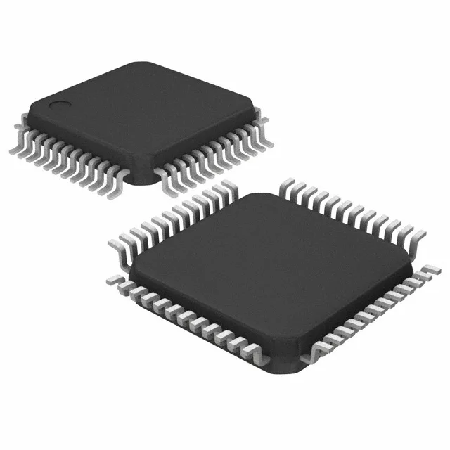
The STM32F103C8T6: ROHS3 compliant per, covering the EU RoHS exemption regime for lead-free assembly.
72 MHz Cortex-M3 — throughput and memory budget
The ARM Cortex-M3 core runs at 72 MHz, the maximum clock for this STM32F103 line — at zero-wait-state from flash, the core delivers 1.25 DMIPS/MHz, so the practical throughput ceiling is about 90 DMIPS before wait states kick in above 24 MHz. On-chip memory: 64 KB of flash (64K x 8) and 20 KB of SRAM (20K x 8). The 64 KB flash holds the application code and constant data; the 20 KB SRAM is the working memory for stack, heap, and DMA buffers. For a typical sensor-node or motor-control firmware with a lightweight RTOS, budget about 8–12 KB for the RTOS kernel and HAL, leaving 8–12 KB for the application heap.
48-LQFP package — PCB footprint and I/O count
That is the full I/O count for this package variant — the 64-pin and 100-pin siblings (STM32F103RFT6, STM32F103VET6) offer 51 and 80 I/O respectively, but require a larger board footprint. Surface-mount assembly: the 0.5 mm pitch demands a 4-layer PCB for reliable fan-out of the inner pins; a 2-layer board can break out only the outer rows.
Supply voltage and temperature — the operating envelope
The internal POR and PDR (programmable voltage detector) monitor the supply; the PVD threshold is set in software to trigger an interrupt before the supply drops below the minimum operating voltage. The internal oscillator and PLL are characterized across this range; the flash read-access timing is compensated by the internal RC oscillator so that wait states are inserted automatically at low temperature when the flash access time exceeds the core clock period.
On-chip peripherals — what connects without external glue
Connectivity interfaces include CANbus (2.0B active), I²C (up to 400 kHz), SPI (up to 18 MHz), USART (up to 4.5 Mbps), and USB 2.0 full-speed (12 Mbps) — all on-chip without external PHY for the USB. The IrDA and LINbus modes share the USART pins. Analog: 10-channel 12-bit successive-approximation ADC with a conversion time as low as 1 µs at 12-bit resolution. The reference voltage is VDD internally — for ratiometric measurements this is fine; for absolute accuracy an external reference on the VREF+ pin (available on the 64-pin and larger packages) is preferred. Motor-control PWM: the advanced-control timer (TIM1) generates up to 6 complementary PWM outputs with dead-time insertion, suitable for 3-phase BLDC or PMSM drives. The DMA controller can transfer ADC results directly to memory without CPU intervention.