Active production — what the lifecycle status means for the BOM line
The STM32F102C8T6: ROHS3 compliant — the part ships lead-free and meets the current EU restriction directive without an exemption. No separate Pb-free conversion date to track.
48 MHz Cortex-M3 — throughput and memory headroom for the firmware engineer
ARM Cortex-M3 core clocked at 48 MHz — this is the STM32F1 value-line speed grade. The 64 KB on-chip flash and 10 KB SRAM leave room for a USB stack and moderate application code; budget the firmware footprint against the 64 KB ceiling before committing the BOM. 37 available I/O in the 48-LQFP package — enough for a parallel LCD data bus, keypad matrix, and a handful of sensor interrupts without needing a port expander.
USB and serial connectivity — peripheral fit for the systems architect
Connectivity includes USB 2.0 Full Speed, two SPI, two I²C, three UART/USART with LIN and IrDA support. The USB peripheral is the main differentiator versus the STM32F103 — the F102 family targets USB-interfaced applications like PC peripherals, game controllers, and USB-to-serial bridges. On-chip peripherals include DMA, a 12-bit ADC with 10 channels, PWM timers, a temperature sensor, and brown-out detection (PDR/POR/PVD). The internal oscillator means the MCU can run without an external crystal for cost-sensitive builds, though USB operation requires a crystal or external clock for accurate bit timing.
48-LQFP footprint and temperature grade — board-fit for the layout engineer
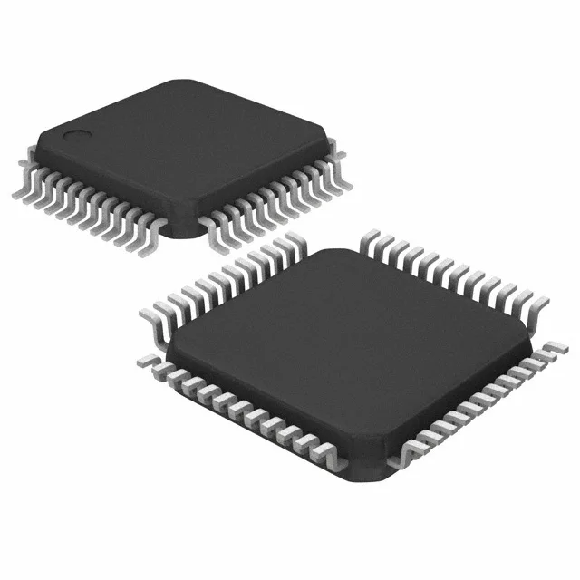
48-LQFP package with 0.5 mm pitch — a two-layer board can route the outer pins, but the inner power and ground pads benefit from a four-layer stack with a dedicated ground plane.
Sourcing posture — how to proceed with the STM32F102C8T6
Active part, no single-source risk from the lifecycle side.