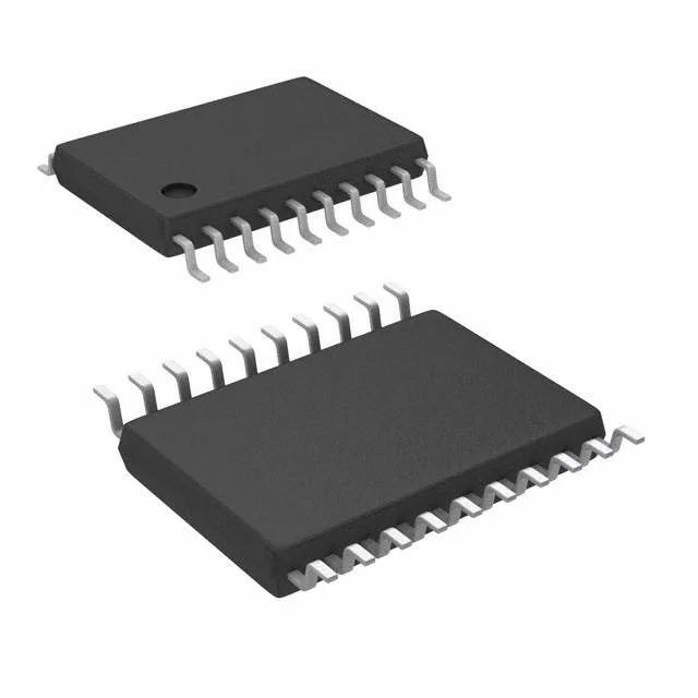
Renesas Electronics 8533AGI-01LFT — Clock & Timing ICs

IDT 8533AGI-01LFT Clock Buffer, 2:4 Fanout, 650 MHz

MPN8533AGI-01LFT
End of Life

IDT 8533AGI-01LFT, Fanout Buffer (Distribution), Multiplexer, 2:4 ratio, 650 MHz max frequency, LVPECL output, accepts CML, HCSL, LVDS, LVHSTL, LVPECL, SSTL inputs, 3.135V-3.465V supply, -40°C to 85°C, 20-TSSOP package.

$14.93Ref. price · indicative, final on quote
Packaging20-TSSOP (0.173", 4.40mm Width)
StockContact for availability
MOQ1 pcs
  • 100% new & originalTraceable channels only — no refurbs, no pulls, no remarked parts.
  • Date & lot codes on quoteStated per line before you commit; label photos on request.
  • MSL-compliant ESD packingMoisture-sealed bags with indicator cards; reels photo-verified.
  • PayPal buyer protectionPay by T/T, PayPal or Payoneer — card payments covered end to end.

Specifications

8533AGI-01LFT Technical Specifications
ParameterValue
TypeFanout Buffer (Distribution), Multiplexer
Mounting typeSurface Mount
Voltage3.135V ~ 3.465V
Frequency650 MHz
Operating temperature-40°C ~ 85°C
InputCML, HCSL, LVDS, LVHSTL, LVPECL, SSTL
OutputLVPECL
PackageTape & Reel (TR); Cut Tape (CT)
Case20-TSSOP (0.173\", 4.40mm Width)
Number of circuits1
Ratio - Input:Output2:4
Differential - Input:OutputYes/Yes

Product details

650 MHz LVPECL fanout buffer with multi-protocol input flexibility

The Renesas (formerly IDT) 8533AGI-01LFT is a 2:4 fanout buffer and multiplexer that accepts six differential input standards — CML, HCSL, LVDS, LVHSTL, LVPECL, and SSTL — and delivers a single LVPECL output at up to 650 MHz. It is a single-circuit device in a 20-TSSOP package, designed for clock distribution in telecom infrastructure, data converters, FPGA reference clock trees, and high-speed backplane applications where a clean LVPECL fanout is needed from a mixed-signal environment.

Input flexibility — the real selection driver

The 2:4 fanout ratio means one input channel can be distributed to four LVPECL loads, or the internal mux selects between two input sources for redundancy or clock-source failover. The wide input protocol support is the differentiating feature: a single BOM line can terminate CML from a SerDes, LVDS from an FPGA, or LVPECL from a high-speed ADC without external level-shifting resistors or translator parts. The 650 MHz ceiling covers gigabit-class SerDes reference clocks and most FPGA transceiver reference frequencies.

3.3V supply — plan the rail budget

The supply range is 3.135 V to 3.465 V, a tight 3.3 V ±5 % window. This is not a wide-range 2.5 V to 5.5 V part; the rail needs to stay clean and within regulation. The differential input-to-output path is fully differential (Yes/Yes), so the part preserves signal integrity through the buffer without single-ended conversion. The industrial temperature range of -40°C to 85°C covers outdoor base stations, motor-drive cabinets, and uncontrolled telecom shelters.

Active lifecycle — no LTB clock ticking

The 8533AGI-01LFT carries an Active product status and ROHS3 compliance. For a production BOM this means no forced redesign cycle from obsolescence; the part can be qualified into new designs with confidence that the supply channel will remain open. The 20-TSSOP footprint is a standard body size (4.40 mm width), shared across the Renesas clock-buffer family, so a layout change for a different fanout ratio or output standard stays pin-compatible across the 20-pin TSSOP variants.

Sourcing this part to your BOM

The 8533AGI-01LFT is sourced through independent distribution channels and quoted to order against an RFQ. For small quantities, the cut-tape option avoids reel minimums.

Frequently asked questions

Is 8533AGI-01LFT compatible with 3.3V logic?

Yes, the supply range is 3.135 V to 3.465 V, which is a standard 3.3 V ±5 % rail. The input accepts CML, HCSL, LVDS, LVHSTL, LVPECL, and SSTL — all common 3.3 V differential signaling standards. No external level translation is needed for those signal types.

What is the maximum frequency of 8533AGI-01LFT?

The maximum frequency is 650 MHz. This covers most FPGA transceiver reference clocks, gigabit Ethernet SerDes, and high-speed ADC/DAC sampling clocks. For applications above 650 MHz, the Renesas 8SLVP1204ANLGI8 family runs to 2 GHz but uses a 20-QFN package.

Can 8533AGI-01LFT replace 8533AGI-01LF?

The 8533AGI-01LFT and 8533AGI-01LF share the same die and electrical specifications. The difference is packaging and shipping format: the -01LFT suffix indicates Tape & Reel packaging, while the -01LF suffix typically ships in tube or tray. Electrically they are identical — same 650 MHz ceiling, same input/output standards, same 20-TSSOP package body. The -01LFT is the reeled variant intended for automated pick-and-place assembly.