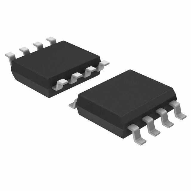
What this part does on the board
The 2305NZ-1HDCG8 is a single-ended LVCMOS fanout buffer from Renesas. It takes one LVCMOS clock input and distributes it to five LVCMOS outputs, buffered and re-driven to maintain signal integrity. The maximum output frequency is 133.33 MHz, which sets the upper bound for the clock tree it feeds — anything faster needs a different buffer or a differential pair like LVPECL. The supply voltage range is 3V to 3.6V, so it sits comfortably on a 3.3V rail. The single-circuit design means one buffer per package; if you need multiple independent fanout groups, you'll use several of these or a multi-circuit part.
That puts this part in indoor, temperature-controlled equipment: office networking gear, telecom racks, test instruments, consumer electronics. Not for outdoor base stations, engine bays, or factory floors where ambient can push past 70°C.
Shipping options include Tape & Reel and Cut Tape.