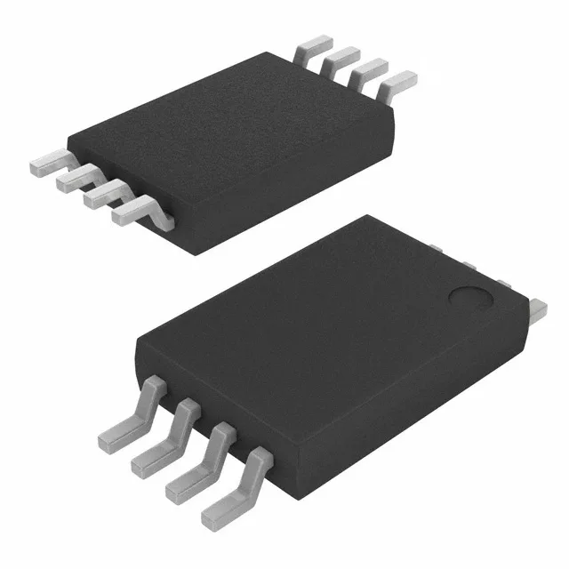
1:4 LVCMOS clock distribution at 200 MHz
The Renesas 5PB1104PGGK is a single-ended fanout buffer that takes one LVCMOS clock input and delivers four LVCMOS outputs with a maximum frequency of 200 MHz. It operates from a wide supply range of 1.71 V to 3.465 V.
The 8-TSSOP package (4.40 mm body width) is a common footprint shared across many Renesas clock fanout parts, so a PCB layout for this part often accepts a pin-compatible sibling without a board spin.
The 1.71 V to 3.465 V operating range covers the three most common logic supply voltages in digital systems.