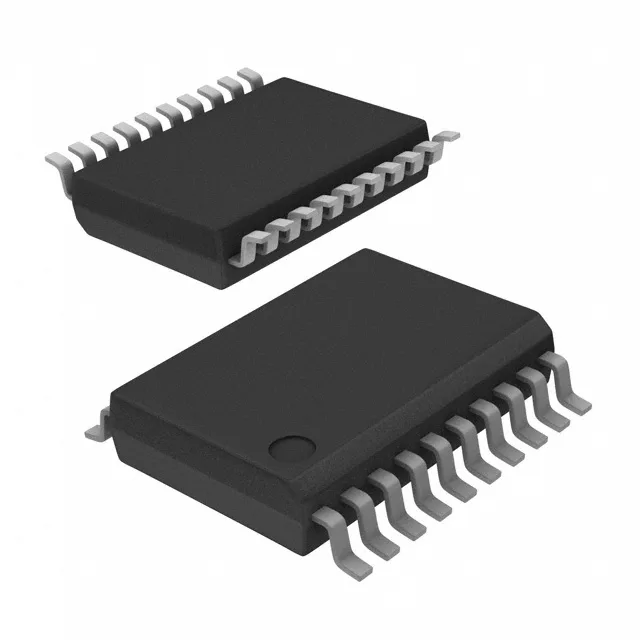
Two-bank fanout buffer for 3.3 V clock trees
The Renesas 49FCT3805EQGI is a non-inverting fanout buffer that takes one CMOS or LVTTL clock input and distributes it to five outputs. Two independent circuits sit in the same 20-QSOP package, so a single device can buffer two separate clock domains or provide redundant fanout for a single source. Input and output levels are both CMOS/LVTTL, meaning it mates directly with 3.3 V logic without level translation.
166 MHz and the 1:5 fanout — what drives the selection
The 166 MHz ceiling is the limiting spec for the clock tree. If your system runs a 100 MHz or 125 MHz reference, this buffer has headroom. Push it near 166 MHz with five loads and the output rise/fall times and duty-cycle distortion become the next constraints — the datasheet's timing tables are the place to check margins. The 1:5 ratio per circuit means one device can feed five loads; with two circuits you get ten total outputs. That density saves board area versus using multiple single-fanout buffers. The non-differential input and output (No/No per the spec) means it is a straight single-ended repeater — not a clock conditioner or a translator to differential standards like LVPECL or LVDS.
20-QSOP — footprint and fit
The 49FCT3805EQGI comes in a 20-lead SSOP body (0.154" wide, 3.90 mm width) and the supplier device package is a 20-QSOP. They share the same footprint — the QSOP is just a thinner version. Surface-mount only. The narrow 3.90 mm width keeps the board footprint small, useful in dense telecom line cards or compact industrial modules. No exposed pad, so thermal management is straightforward — just standard FR-4 copper pours.