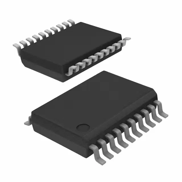
What this 49FCT3805AQG8 clock buffer does on the board
The Renesas 49FCT3805AQG8 is a fanout buffer — it takes one clock input and splits it to five outputs, cleanly, without the jitter or skew you get from daisy-chaining gates. Two independent 1:5 banks live in the same 20-QSOP package, so a single part can distribute two separate clock domains across ten loads. Input and output levels are CMOS and LVTTL, meaning it talks directly to the 3.3 V logic on your board without external translation. Supply range is 3 V to 3.6 V, which locks it into 3.3 V systems — not a 5 V or 1.8 V part.
Having two independent 1:5 buffers in one package saves board space and trace length. Each bank has its own input and five outputs, so you can feed a 25 MHz reference to five FPGA banks on one side and a 100 MHz Ethernet clock to five PHYs on the other, all from the same IC. The non-differential I/O (No/No) means this is a single-ended clock distribution part — no PECL or LVDS outputs, so keep it for standard CMOS/LVTTL fanout.
Package and footprint notes for the rework bench
The 20-QSOP (0.154", 3.90 mm width) is a narrow-body SSOP derivative. It is surface-mount only, so no socket for field swapping — you will need a hot-air station or a fine-tip iron and some patience. The body is small enough that orientation marking is usually a pin-1 dot on top; check it under a loupe before placing. MSL is not in the record, but a common-sense bake at 125°C for 8 hours if the moisture-barrier bag is compromised is cheap insurance.