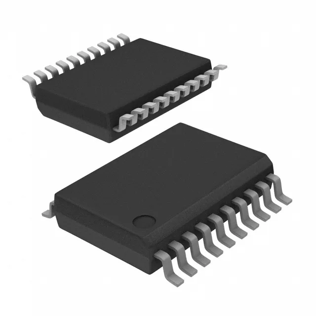
Two 1:5 buffers in one 20-SSOP package
The Renesas 49FCT20805PYGI is a fanout buffer (distribution) IC that packs two independent 1:5 clock or signal buffers into a single 20-SSOP package. Each buffer takes one CMOS or LVTTL input and drives five CMOS or LVTTL outputs, giving you a total of ten outputs from two inputs. The part is non-differential on both input and output sides, so it is a straight single-ended fanout tree for standard logic-level clocks or data strobes.
The 166 MHz maximum frequency covers the vast majority of board-level clock distribution for FPGAs, MCUs, and Ethernet PHYs running at 100 MHz or below. If your design needs to fan out a 125 MHz reference or a 100 MHz system clock, this part has margin. The supply voltage range of 2.3 V to 2.7 V locks it into 2.5 V nominal rails — it will not run from 3.3 V or 1.8 V without a regulator.