1:5 fanout, two circuits — what you get
The 49FCT3805APYGI is a non-inverting clock buffer from Renesas's 49FCT series. It takes one CMOS or LVTTL input and distributes it to five outputs per circuit, with two independent circuits on the die — so a single package can drive ten clock loads from two separate sources. The input-to-output ratio is 1:5 per circuit, and the part is non-differential (single-ended in, single-ended out). This is a straight fanout buffer, not a PLL or zero-delay buffer — no skew adjustment, no frequency multiplication. It is meant for cleanly rebuffering a clock or data strobe to multiple loads on the same board.
3.3 V only — plan the rail
Supply range is 3 V to 3.6 V, which is the 3.3 V ±10 % window. If your system runs a 1.8 V or 2.5 V core logic, this buffer needs its own 3.3 V rail or a level translator on the input. The I/O is CMOS/LVTTL, so it will accept 3.3 V CMOS levels directly and drive the same. No differential I/O here — single-ended only, which keeps the pin count low but limits noise immunity on long traces.
Industrial temperature, surface-mount SSOP
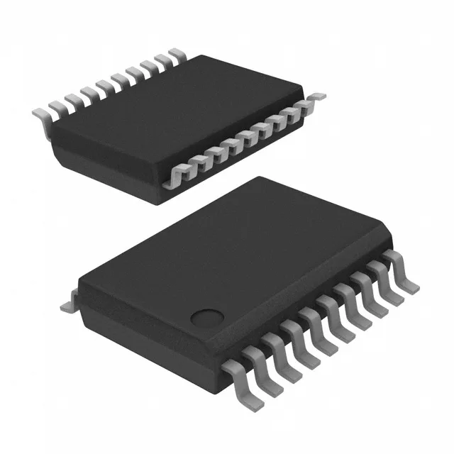
The package is a 20-pin SSOP, 5.30 mm body width, surface-mount. No exposed pad — all dissipation goes through the leads, so keep the ambient airflow reasonable if you are running all ten outputs near the supply maximum.
Active, ROHS3, no end-of-life concern
ROHS3 compliant, so it passes EU and California restrictions without exemption paperwork. The 49FCT series is a mature logic family, but Renesas continues to support it for industrial clock-tree designs. No official second source is listed in the record, but the part is widely available through independent distribution.