Two independent 1:5 fanout paths for 3.3V clock trees
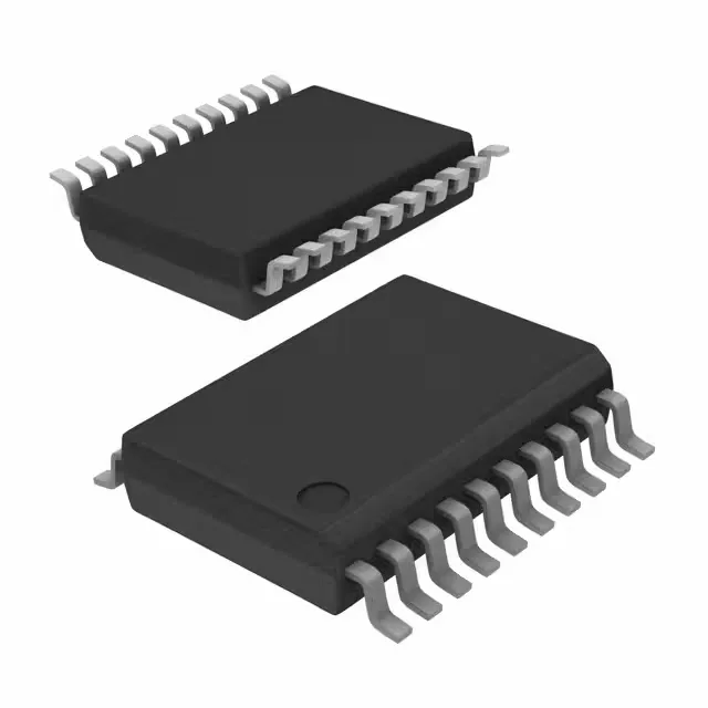
The 49FCT3805AQG is a Renesas fanout buffer with two independent circuits, each splitting one input into five outputs — ten total from two inputs. This part fits 3.3V clock distribution where you need separate buffered copies of two clock sources, like splitting a reference clock to multiple PLLs or ASICs on the same board.
Single-ended IO limits the signal-integrity budget
Both input and output are non-differential (No/No), so the part cannot reject common-mode noise the way an LVPECL or LVDS buffer does. For long traces or noisy environments, the 49FCT3805AQG needs careful layout — keep the trace impedance controlled and the return path short. Compare with the 8SLVP1104ANLGI, which offers differential LVPECL outputs at 2 GHz but runs a single circuit at 1:4 ratio and needs a 3.135V supply. The 49FCT3805AQG gives you two circuits at 1:5 but tops out at lower frequency and lacks differential drive.
That's a common footprint — the 0.025-inch pitch QSOP is widely second-sourced.
Commercial temp grade — keep it indoors
Not for outdoor, under-hood, or extended-temperature industrial use.