What the 750 MHz and 1:12 fanout mean for your clock tree
The ZL30237GGG2 is a non-PLL clock buffer that distributes a single reference clock or crystal input to twelve independent outputs, each capable of up to 750 MHz in LVCMOS or LVPECL format. Because there is no PLL, the output frequency equals the input frequency with a fixed propagation delay — no jitter accumulation from a VCO, but also no frequency multiplication. This makes it a deterministic fanout buffer for distributing a clean reference across a board, not a synthesizer.
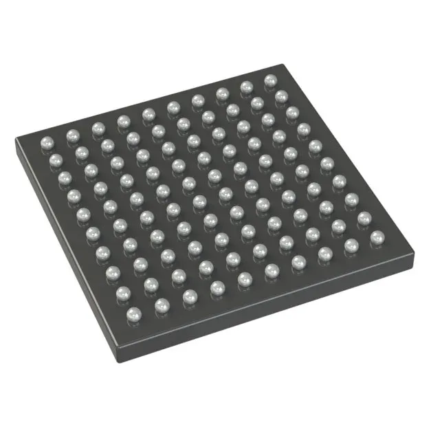
Package and board integration — 100-LBGA layout demands
The 100-ball LBGA measures 11x11 mm with a 0.80 mm ball pitch. Routing twelve high-speed outputs at 750 MHz requires impedance-controlled traces, preferably on an inner layer with continuous ground reference, and via-in-pad or microvia fan-out under the BGA to keep stub lengths short. The differential outputs (LVPECL) need 100-ohm differential trace pairs; the single-ended LVCMOS outputs need 50-ohm controlled impedance to the load. Both output types share the same 12 output pins — each pair can be configured per bank.
Target interfaces and temperature range
This buffer is specified for Ethernet, Fibre Channel, memory and PCI Express timing domains — the four synchronous interface families that share a common reference clock architecture and benefit from a low-jitter, deterministic fanout. The 100-LBGA package is RoHS3 compliant per the active lifecycle status.
Active lifecycle and compliance documentation
Microchip continues to support this part for new designs and production BOMs. RoHS3 compliance is confirmed. The manufacturer provides the standard compliance documentation (RoHS declaration, REACH SVHC statement, material declaration) upon request through the supply chain.