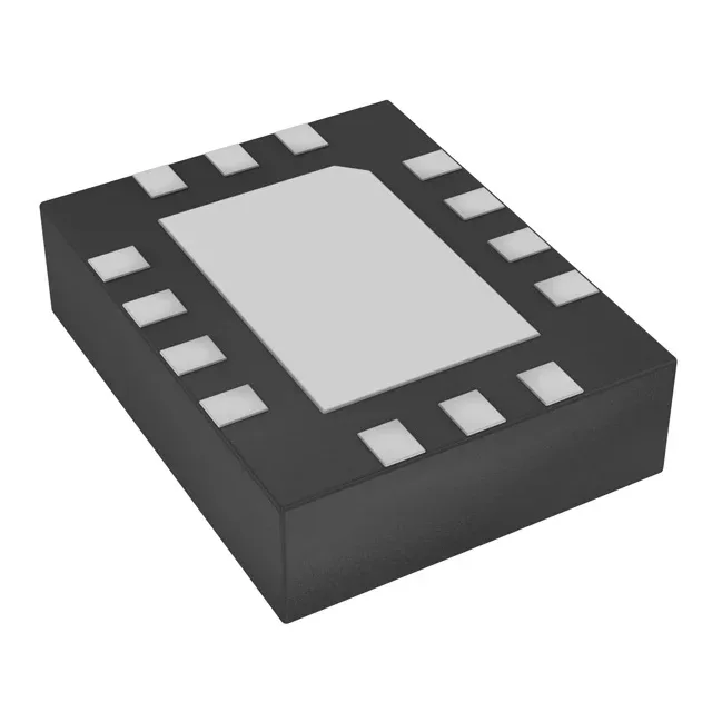
Microchip Technology DSC557-053344KL1T — Clock & Timing ICs

Microchip DSC557-053344KL1T PCIe Clock Gen, 100MHz

MPNDSC557-053344KL1T
Active

Microchip Technology DSC557-05 series PCI Express (PCIe) clock generator, integrated PLL, 100 MHz max, HCSL/LVDS outputs, 20-VFQFN exposed pad, 2.25V~3.6V supply, -40°C~105°C.

$6.1050Ref. price · indicative, final on quote
Packaging20-VFQFN Exposed Pad
RoHSROHS3 Compliant
SeriesDSC557-05
Independent supplier — new & surplus stockAuthenticity-screened · ESD-safe packingListing updated Aug 2026

Specifications

DSC557-053344KL1T specifications
ParameterValue
SeriesDSC557-05
MountingSurface Mount
Voltage2.25V ~ 3.6V
Frequency100MHz
Operating temperature-40°C~105°C
PLLYes
OutputHCSL, LVDS
PackageTape & Reel (TR); Cut Tape (CT)
Main purposePCI Express (PCIe)
Case20-VFQFN Exposed Pad
Number of circuits1
Ratio - Input:Output0:4
Differential - Input:OutputNo/Yes

Product details

PCIe reference clock with integrated PLL

The DSC557-053344KL1T is a PCI Express (PCIe) clock generator from Microchip's DSC557-05 series, built around an integrated PLL to synthesize a clean 100 MHz reference clock from an internal or external source. The PLL locks to the input and generates four differential outputs in either HCSL or LVDS format, covering the two most common signaling standards for PCIe reference clocks. Because the input-to-output ratio is 0:4, this part accepts no single-ended input — it expects a differential reference or uses an internal oscillator. The differential outputs mean the receiver sees a low-jitter, common-mode-rejected clock edge, which is essential for PCIe Gen1/2/3 link stability where the reference clock jitter budget is tight.

Supply, temperature, and package fit

The exposed pad also provides a low-inductance return path for the high-speed output currents — a layout detail that matters when routing the HCSL or LVDS traces to the PCIe slot or endpoint.

The part is RoHS3 compliant, which means it meets the EU RoHS exemption-free standard for lead, mercury, cadmium, and other restricted substances, so it ships without a RoHS exemption statement.

Frequently asked questions

What output standards does the DSC557-053344KL1T support?

The part outputs HCSL and LVDS — both differential standards. HCSL is the traditional PCIe reference clock format, while LVDS offers lower swing and lower power for some chipset or FPGA clock inputs. The output format is selected via the device's configuration pins or strapping.

What is the maximum operating frequency of the DSC557-053344KL1T?

The maximum output frequency is 100 MHz, which is the standard PCIe reference clock speed. The integrated PLL locks to the input and multiplies it to this frequency.