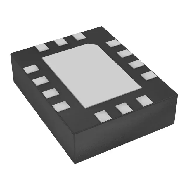
PCIe reference clock in a 14-QFN package
The DSC557-0343FI0 is a PLL-based clock generator from Microchip's DSC557-03 series, purpose-built for PCI Express (PCIe) reference clock generation. It delivers two differential outputs configurable as HCSL or LVDS, with a maximum output frequency of 100 MHz — the standard reference clock rate for PCIe Gen1, Gen2, and Gen3 lanes. The 0:2 input-to-output ratio means there is no reference input pin; the internal PLL synthesises the clock from an on-chip MEMS resonator, eliminating the need for an external crystal or oscillator. This simplifies the BOM and saves board area in space-constrained designs like add-in cards, mini-PCIe modules, and embedded systems.
Supply voltage and temperature grade
The differential output stage (No/Yes for input/output) means the outputs are always differential — HCSL or LVDS — while the input side is single-ended. This suits PCIe clock distribution where the reference clock must be differential from the source to the endpoint.
Housed in a 14-VFQFN exposed-pad package (2.5 mm × 3.2 mm body), the DSC557-0343FI0 occupies minimal PCB area.
Active lifecycle and sourcing
The base product number DSC557 covers multiple output frequency and configuration variants; the -0343 suffix encodes the specific 100 MHz HCSL/LVDS option. No pin-compatible second source is listed in the ledger, but the DSC557-03 series shares the same footprint across frequency options, simplifying last-minute BOM swaps if a different frequency is needed.