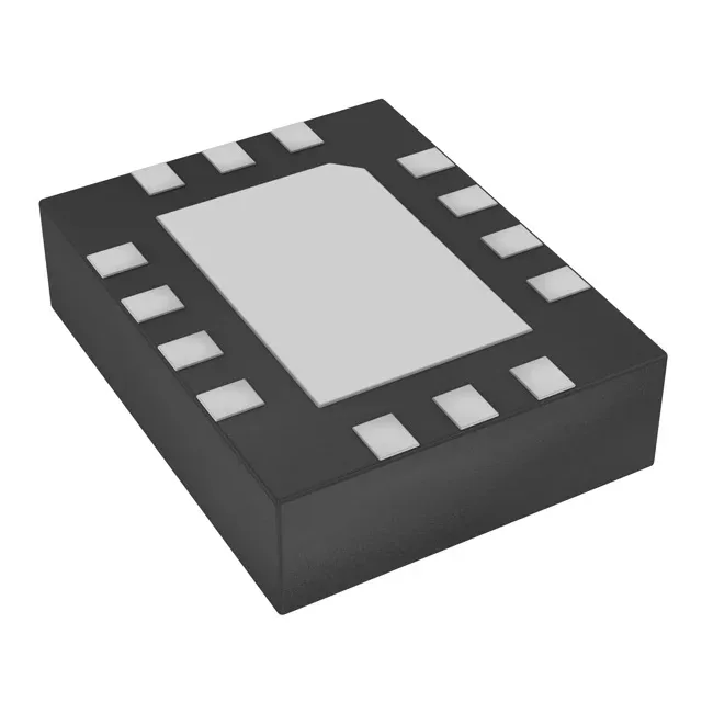
Microchip Technology DSC557-0344FI0T — Clock & Timing ICs
Technical Documents PDF / CAD
RoHS Compliant · Lead-Free EIA-481 Standard
Microchip Technology / Clock & Timing ICs

DSC557-0344FI0T Microchip PCIe Clock Gen, 100MHz HCSL

MPN DSC557-0344FI0T
Active Spot Stock · 24-48h Dispatch 100% Original Sealed

Microchip Technology DSC557-03 series PCI Express (PCIe) clock generator, DSC557-0344FI0T, 100 MHz max, HCSL output, PLL Yes, 2.25V~3.6V supply, -40°C~85°C, 14-VFQFN Exposed Pad, Surface Mount.

In Stock: 1,000 pcs
MOQ: 1 pcs
Logistics: DHL / FedEx DAP (Global Express · 3-7d) Russia & CIS DDP (Door-to-Door Cleared)
Dispatch: Shenzhen / HK
Unit Price (USD)
$2.94 / pc
Direct Purchase Ready
Volume Pricing Breaks Confirmed upon quotation
1+ pcs
$2.94
10+ pcs
$2.65
30+ pcs
$2.41
100+ pcs
$2.18
500+ pcs
$2.03
1,000+ pcs
$1.91
Working on a production BOM or have a target unit price? Submit Target Price
Buy Now

$2.94 / ea

1,000 in stock — maximum per order · 3–4 days lead time

$2.65 / ea from 10 pcs

Upload Full BOM List
[SPEC] Essential Parameters Snapshot Full Specifications (13)
Package / Case 14-VFQFN Exposed Pad
Supply Voltage 2.25V ~ 3.6V

Full Technical Specifications

13 Parameters
DSC557-0344FI0T specifications
Parameter / AttributeSpecification / Value
SeriesDSC557-03
MountingSurface Mount
Supply voltage2.25V ~ 3.6V
Frequency - max100MHz
Operating temperature-40°C~85°C
PLLYes
OutputHCSL
PackageTape & Reel (TR); Cut Tape (CT)
Main purposePCI Express (PCIe)
Case14-VFQFN Exposed Pad
Number of circuits1
Ratio - Input:Output0:2
Differential - Input:OutputNo/Yes
Series Sibling Variants

Microchip Technology DSC557-03 Series Models

Sibling variants, package options, and speed/density grades in this Microchip Technology semiconductor series. Active Shenzhen warehouse allocation and rapid 24-48h dispatch.

Technical Details & Description

PCIe reference clock with integrated PLL

The DSC557-0344FI0T is a PCI Express (PCIe) clock generator from Microchip Technology's DSC557-03 series, delivering a 100 MHz HCSL differential output from a single-ended input — the standard topology for PCIe Gen1, Gen2, and Gen3 reference clocks. The integrated PLL synthesises the output without an external VCXO or crystal, reducing BOM count on the clock tree. The 0:2 input-to-output ratio means it accepts one reference and drives two HCSL lanes — enough for a root complex and one endpoint on the same clock domain.

Frequently asked questions

What is the output type and maximum frequency of DSC557-0344FI0T?

The output is HCSL at a maximum frequency of 100 MHz. This matches the PCIe reference clock requirement for Gen1, Gen2, and Gen3 base clocks.

DSC557-0344FI0T
Verified Allocation
Quote