72 Mbit synchronous SRAM at 200 MHz — the throughput ceiling
The CY7C1470BV25-200BZXI: This is a 72 Mbit synchronous SRAM organized as 2M words x 36 bits. The 200 MHz clock frequency sets the maximum data rate on the parallel bus — each clock edge latches a 36-bit word, so the raw bandwidth is 200 million 36-bit transfers per second. The 3 ns access time is the time from the address being valid to the data appearing on the output pins; it determines the read-cycle timing margin for the memory controller or FPGA interface. The memory uses a synchronous SDR (single-data-rate) architecture with a parallel interface. That means the address, control, and data lines all transition on the rising edge of the clock — no DDR-style double-pumping. The controller must meet the setup and hold times relative to that single edge; the 200 MHz clock period of 5 ns leaves 2 ns of margin after the 3 ns access time for the data to propagate to the receiver.
Industrial temperature and 165-ball FBGA — the board-fit constraints
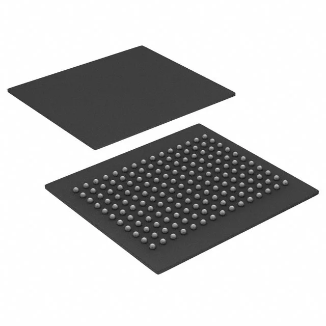
The 165-ball FBGA package has a 15x17 mm body. The ball pitch is 1.0 mm, which is a standard four-layer PCB fan-out; the centre thermal pad must be connected to the ground plane with at least nine thermal vias to keep the junction temperature below the 85°C limit under sustained 200 MHz operation. The supply voltage is 2.375 V to 2.625 V, a tight 250 mV window around the nominal 2.5 V rail. The power tree must regulate to within ±5 % at the FBGA balls — a 2.5 V LDO with 1 % accuracy and 50 mV dropout at the full 500 mA load current is a safe starting point. The core and I/O share the same supply; there is no separate Vddq rail.