Clock driver with PLL bypass — what it does on your board
The CY29350AIT is a single-circuit clock driver that takes one LVCMOS or LVTTL input and fans it out to nine LVCMOS outputs, with a PLL that can be bypassed. Maximum output frequency is 200 MHz. Supply range is 2.375 V to 3.465 V.
Industrial temperature range — field-fit without a mil-grade premium
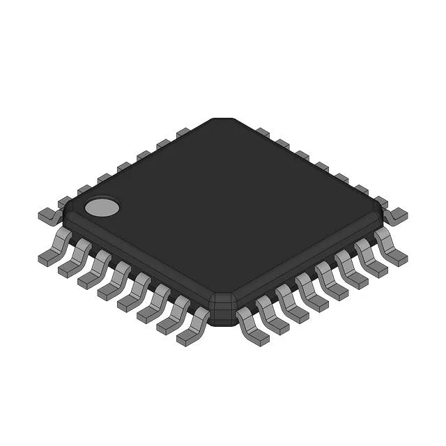
The 32-TQFP package (7x7 mm) is a common footprint, so board layout and rework are straightforward — no hot-air station required for a field swap if the board is accessible.
Lifecycle — active, no LTB clock ticking
That means you can commit this part to a BOM without worrying about a last-time-buy window closing. RoHS non-compliant per the listing — check your assembly line's exemption policy if you need lead-free.