PLL with bypass — glitch-free clock switching
The CY29350AI integrates a PLL with a bypass path, meaning the output can switch between a multiplied clock and a clean feed-through of the reference without re-lock transients — useful when a system must fall back to a free-running oscillator during PLL failure or test mode.
200 MHz fan-out, 2:9 ratio
Rated for a maximum output frequency of 200 MHz, this clock driver accepts LVCMOS or LVTTL inputs and delivers nine LVCMOS outputs from two input lines — a 2:9 fan-out that suits distributing a master clock to multiple ASICs or FPGAs on a single board.
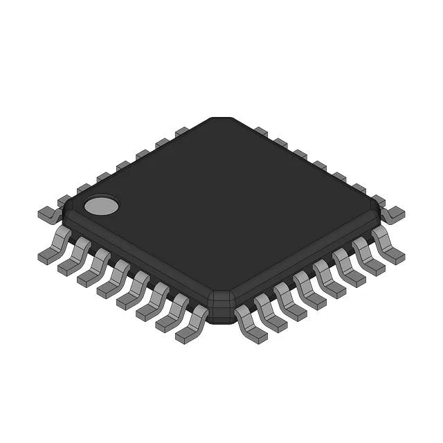
32-TQFP — layout and sourcing
The 0.8 mm pitch fan-outs on two-layer boards without microvias, and the exposed paddle (if present) should be tied to the ground plane for thermal relief.