What this 2:12 fanout buffer does for a high-speed clock tree
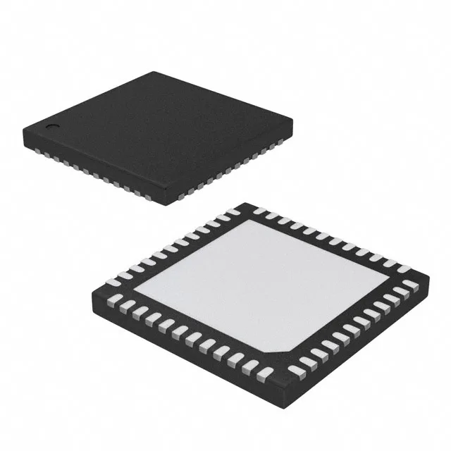
The ADCLK854BCPZ-REEL7 is a 2:12 fanout buffer and multiplexer from Analog Devices that takes one or two clock inputs and distributes them to twelve outputs at frequencies up to 1.2 GHz. It accepts any of five common signal standards — CML, CMOS, HSTL, LVDS, LVPECL — on the input side and delivers CMOS or LVDS-level outputs. This universal input compatibility means you can route a single clock source (say, a 156.25 MHz LVDS oscillator for 10GbE) directly into the part without external level translators, then fan it out to twelve destinations such as FPGA transceivers, SERDES, or ADCs. The part is built for industrial environments with a -40°C to 85°C operating range, and it runs from a 1.8V nominal supply (1.71V to 1.89V), which matches the core voltage of many modern FPGAs and ASICs.
The 1.2 GHz maximum frequency covers the common telecom and data-center clock rates: 125 MHz (GbE), 156.25 MHz (10GbE), 312.5 MHz, 625 MHz, and even 1.25 GHz for some SERDES reference clocks. At these speeds, the differential input-to-output path (Yes/Yes per the datasheet) preserves signal integrity by rejecting common-mode noise. The 2:12 ratio lets you replace two 1:6 fanout buffers with a single device, saving board area and reducing the number of clock-tree components that can accumulate jitter.
The part is ROHS3 compliant. If you are comparing with the ADCLK846BCPZ-REEL7, note that the 846 is a 1:6 fanout (half the output count) but otherwise shares the same 1.2 GHz speed, input standards, and package footprint — a viable second source for lower-density applications.