Clock recovery for STS-1 — what this part does
The 1:2 input-to-output ratio means it can fan out the recovered clock to two destinations — useful for driving a line interface and a local framer simultaneously.
ECL I/O — plan the logic interface
Both input and output are ECL levels. That is the key interface constraint: the downstream receiver must accept ECL swings, or you need a level translator (e.g., to PECL or LVPECL) if your framer or FPGA bank runs on a different standard. The differential I/O path (Yes/Yes) gives common-mode rejection on the backplane — helpful in a telecom shelf where ground bounce between cards is a real concern.
Industrial temperature range, active lifecycle
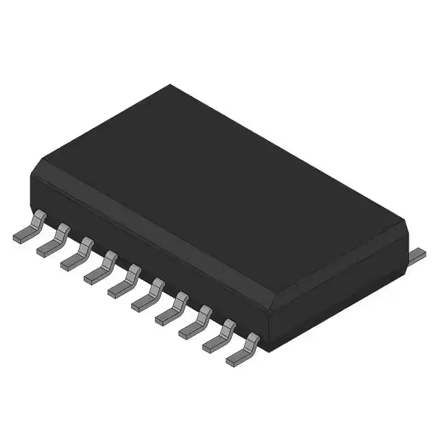
20-SOIC footprint — board layout note
Housed in a 20-SOIC wide-body (7.50 mm width), surface-mount.