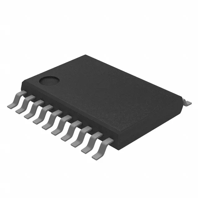
Toshiba Semiconductor 74LCX373FT — Discrete Semiconductors
Technical Documents PDF / CAD
RoHS Compliant · Lead-Free EIA-481 Standard
Toshiba Semiconductor / Discrete Semiconductors

Toshiba 74LCX373FT D-Type Transparent Latch, 1.5ns, 20-TSSOP

MPN 74LCX373FT
End of Life Spot Stock · 24-48h Dispatch 100% Original Sealed

Toshiba Semiconductor TC74LCX series D-Type Transparent Latch, 8:8 circuit, Tri-State output, 1.65V-3.6V supply, 1.5ns propagation delay, 24mA output drive, -40°C to 85°C, 20-TSSOP package, Tape & Reel.

In Stock: 48 pcs
MOQ: 1 pcs
Logistics: DHL / FedEx DAP (Global Express · 3-7d) Russia & CIS DDP (Door-to-Door Cleared)
Dispatch: Shenzhen / HK
Unit Price (USD)
$0.65 / pc
Direct Purchase Ready
Volume Pricing Breaks Confirmed upon quotation
1+ pcs
$0.65
10+ pcs
$0.51
30+ pcs
$0.46
Working on a production BOM or have a target unit price? Submit Target Price
Buy Now

$0.65 / ea

48 in stock — maximum per order · 3–4 days lead time

$0.51 / ea from 10 pcs

Upload Full BOM List
[SPEC] Essential Parameters Snapshot Full Specifications (12)
Package / Case 20-TSSOP (0.173", 4.40mm Width)
Supply Voltage 1.65V ~ 3.6V
Output / Current 24mA, 24mA

Full Technical Specifications

12 Parameters
74LCX373FT specifications
Parameter / AttributeSpecification / Value
SeriesTC74LCX
Logic typeD-Type Transparent Latch
Output typeTri-State
MountingSurface Mount
Supply voltage1.65V ~ 3.6V
Current - output high, low24mA, 24mA
Operating temperature-40°C ~ 85°C
Circuit8:8
PackageTape & Reel (TR)
Case20-TSSOP (0.173\", 4.40mm Width)
Independent circuits1
Delay time - propagation1.5ns
Series Sibling Variants

Toshiba Semiconductor TC74LCX Series Models

Sibling variants, package options, and speed/density grades in this Toshiba Semiconductor semiconductor series. Active Shenzhen warehouse allocation and rapid 24-48h dispatch.

Technical Details & Description

1.5 ns propagation delay — 8-bit transparent latch for low-voltage buses

The Toshiba 74LCX373FT is an 8-bit D-type transparent latch with tri-state outputs, part of the TC74LCX series. The 1.5 ns propagation delay sets the timing margin for the data path — at a 100 MHz bus cycle (10 ns period), 1.5 ns consumes 15% of the cycle, leaving 8.5 ns for setup, hold, and clock-to-output of the driving and receiving devices. This delay is specified at the 1.65 V low end of the supply range; at 3.3 V the delay is typically shorter, but the 1.5 ns max figure is the one to budget in worst-case timing analysis. The tri-state outputs let multiple latches share a common data bus — the high-impedance state eliminates contention when the latch is not selected.

The supplier device package is 20-TSSOP — the same body as the package/case, so the footprint is consistent across the datasheet and the assembly house's library. The 8:8 circuit configuration means eight data inputs map to eight outputs — one independent latch per bit. The single independent circuit confirms that all eight latches share a common enable and output-enable control, simplifying the control logic.

Active lifecycle — sourcing posture

For a low-voltage 8-bit latch in a 20-TSSOP package, the 74LCX373FT is a drop-in candidate for designs using the TC74LCX family.

Frequently asked questions

What is the propagation delay of 74LCX373FT and why does it matter?

The propagation delay is 1.5 ns maximum at 1.65 V supply. This is the time from the latch-enable edge to the output changing state. At a 100 MHz bus cycle (10 ns), 1.5 ns leaves 8.5 ns for the rest of the timing path — setup, hold, and clock-to-output of adjacent devices. Budget this worst-case delay in your timing closure analysis.

74LCX373FT
Verified Allocation
Quote