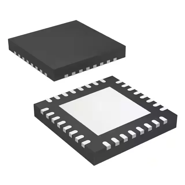
Four-output PCIe/clock buffer for automotive timing trees
It accepts a wide range of differential and single-ended input standards — CML, HCSL, HSTL, LVDS, LVPECL, SSTL, or a crystal — and outputs HCSL or LVCMOS levels. The 3:5 input-to-output ratio and fully differential signal path let it fan out a clean reference clock to multiple PCIe or SATA endpoints without adding a PLL (this is a fanout buffer, not a jitter cleaner). Rated across -40 to 105°C and AEC-Q100 qualified, it suits under-hood ECUs, infotainment head units, and ADAS sensor fusion boards where a single master clock must reach several receivers with matched skew.
400 MHz bandwidth and input flexibility
The 400 MHz maximum frequency covers PCIe Gen 1 through Gen 3 reference clocks and most SATA/SAS base rates. Because the part has no internal PLL, it passes through the input phase noise unmodified — the system clock source must already meet the jitter budget. The input stage accepts LVPECL, HCSL, LVDS, HSTL, CML, SSTL, or a crystal oscillator, which means a single BOM line can bridge between a legacy LVPECL oscillator and an HCSL fan-out tree without level translators. The 3:5 ratio gives three independent input banks that can be selected via control pins, useful for redundant clock sources or multi-protocol test modes.
It is ROHS3 compliant and part of TI's automotive-qualified portfolio.