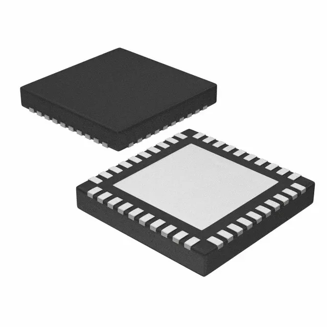
Active BLE SoC with 256 kB Flash — still a production-ready BOM line
The Texas Instruments CC2540F256RHAR is a single-chip Bluetooth 5.0-compliant SoC integrating a 2.4 GHz transceiver and an 8051-based MCU core.
21 GPIO and serial interfaces — peripheral headroom for sensor nodes
With 21 GPIO lines and support for SPI, USART, and USB serial interfaces, this SoC can handle multiple sensors, a display, and a host link without an external I/O expander. The 8 kB SRAM is the tight spot — enough for BLE data buffers and a small state machine, but not for heavy data logging. Firmware teams should budget the stack's RAM footprint early.
Supply range and current draw — battery-driven design fit
Receiving current is 19.6 mA to 22.1 mA; transmitting at 4 dBm output draws 21.1 mA to 31.6 mA. Those numbers are typical for a BLE SoC of this generation — budget for peak TX current in the power supply design and battery life calculations.
40-VFQFN package — thermal and layout notes
The exposed pad is the ground return — connect it to a solid ground plane with at least four vias. Surface-mount assembly is standard; no special reflow profile beyond the usual lead-free ramp.
Sensitivity and output power — link budget reality
Receiver sensitivity is rated at -93 dBm, and the maximum transmit power is 4 dBm. That gives a raw link budget of about 97 dB — enough for tens of meters indoors with a good antenna. The 1 Mbps data rate is the standard BLE GFSK rate; no 2 Mbps PHY is supported. For range-critical designs, the -93 dBm figure is competitive with other BLE 4.x/5.0 parts.