23 GPIO — what you can actually connect
With 23 GPIO lines, this chip can handle a handful of sensors, an SPI or I²C display, and still leave pins for button inputs and status LEDs. The serial interfaces include I²C, SPI, and USART, so hooking up a MEMS accelerometer or a temperature sensor over I²C is straightforward — no need for an external bridge. Just remember that some of those GPIOs double as analog inputs or debug lines; check the pin mux before committing the schematic.
Receiver sensitivity and link budget
The -99 dBm sensitivity (typical) gives a usable link budget around 99 dB when paired with the 0 dBm transmit output. In a clean indoor environment that translates to roughly 50–80 meters line-of-sight, though walls and metal shelving will knock that down. For a wearable or a home-automation sensor that stays within the same room, the margin is plenty; for a warehouse asset tracker, plan for a mesh or a higher-output front end.
Lifecycle — still active, no LTB looming
The base product number is CC2541, so any PCN or errata updates will carry that prefix.
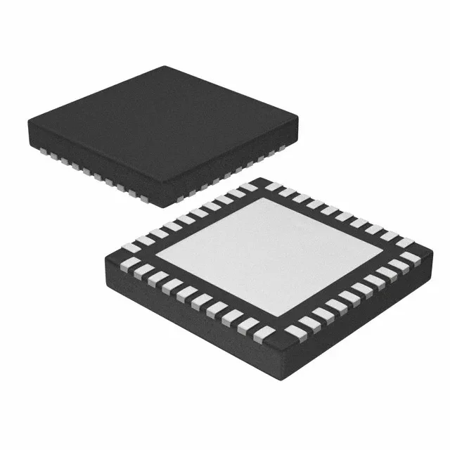
Rework note — 40-VFQFN with exposed pad
The 40-VFQFN package (6x6 mm, 0.5 mm pitch) is reworkable with a hot-air station if you have a decent preheat plate under the board. Bake the board at 125 °C for 24 hours if the moisture-barrier bag has been open longer than the floor-life window — MSL 3 parts can pop if you hit them with hot air without drying first.